Perovskite-Info: the perovskite experts

Perovskite-Info is a news hub and knowledge center born out of keen interest in the wide range of perovskite materials.

Perovskites are a class of materials that share a similar structure, which display a myriad of exciting properties like superconductivity, magnetoresistance and more. These easily synthesized materials are considered the future of solar cells, as their distinctive structure makes them perfect for enabling low-cost, efficient photovoltaics. They are also predicted to play a role in next-gen electric vehicle batteries, sensors, lasers and much more.

Recent Perovskite News

Researchers develop flexible quasi-2D perovskite solar cells with high specific power and improved stability for energy-autonomous drones

Researchers at Austria's Johannes Kepler University Linz have developed lightweight, thin (<2.5 μm), flexible and transparent-conductive-oxide-free quasi-two-dimensional perovskite solar cells by incorporating alpha-methylbenzyl ammonium iodide into the photoactive perovskite layer. 

The team fabricated the devices directly on an ultrathin polymer foil coated with an alumina barrier layer to ensure environmental and mechanical stability without compromising weight and flexibility. 
Read the full story Posted: Apr 21,2024

Researchers highlight the potential of ambient air annealing for efficient inorganic CsPbI3 perovskite solar cells

Researchers from Helmholtz-Zentrum Berlin (HZB) and the University of Potsdam have analyzed surfaces and interfaces of CsPbI3 films, produced under different conditions, at BESSY II. They found that annealing in ambient air does not have an adverse effect on the optoelectronic properties of the semiconductor film, but actually results in fewer defects. This could simplify the mass production of inorganic perovskite solar cells.

The best performing perovskite semiconductors contain organic cations such as methylammonium, which cannot tolerate high temperatures and humidity, so their long-term stability is still a challenge. However, methylammonium can be replaced by inorganic cations such as Cesium (Cs). Inorganic halide perovskites with the molecular formula CsPbX3 (where X stands for a halide such as chloride, bromide and iodide) remain stable even at temperatures above 300 °C. CsPbI3 has the best optical properties for photovoltaics (band gap ∼1.7 eV).

Read the full story Posted: Apr 20,2024

KEP Technologies develop perovskites-based radiation detection devices

Halide perovskite single crystals such as MAPbBr3 or CsPbBr3 possess properties that make them particularly interesting for the detection of ionizing radiation. The most important of these are their high stopping power for absorbing gamma rays, their low-dark current and effective-charge-transport capability. They are therefore ideal for efficiently producing charges when gamma rays pass through them, which is a basic function required for their use in a detection device.

KEP Technologies, through its Setsafe brand, is developing prototype-level radiation detection devices that incorporate halide perovskite single crystals and that can trigger an alarm based on various criteria. These devices target applications for defense and public protection against nuclear and radiological risks.

Read the full story Posted: Apr 19,2024

Researchers develop novel vapor deposition technique based on continuous flash sublimation for rapid fabrication of all-inorganic perovskite solar cells

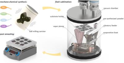
Researchers at NREL, BlueDot Photonics, University of Washington, Colorado School of Mines and Rochester Institute of Technology have developed a vapor deposition technique based on continuous flash sublimation (CFS) to fabricate all-inorganic perovskite thin films in under 5 minutes in a continuous process. The adoption of the proposed approach may also result in higher power conversion efficiencies of perovskite solar cell.

Schematic illustration of the continuous flash sublimation (CFS) approach consisting of a mechano-chemical synthesis of the source powder (here CsPb(IxBr1−x)3), the high-throughput deposition process in a home-made evaporation system, and a short post-annealing treatment to improve thin-film quality. Image from Journal of Materials Chemistry A

The team described the new technique as a non-batch process that solves two problems associated with the use of established vapor processing in perovskite material manufacturing – the slow speed of deposition and the non-continuous nature of batch processing.

Read the full story Posted: Apr 18,2024

Perovskites’ bright future in the MicroLED industry

Micro-LED (also known as mLED or µLED) is a display technology based on miniature LED devices that are used to directly create color pixels. Micro-LED displays are highly promising and have the potential to create efficient and great looking flexible displays, which could challenge even the most impressive high-end OLED displays. Micro LEDs are attracting significant attention as next-generation displays owing to their desirable characteristics such as low power consumption, high contrast ratio, high brightness, fast response speed, and long life span.

Samsung Electronics 89-inch microLED TV, 2023

Perovskite materials can benefit the MicroLED industry in two ways: as materials for color conversion (using perovskite-based QDs) and in perovskite-based LED emitters. Much R&D work is taking place on both these fronts, and interest seems to be growing.

Read the full story Posted: Apr 16,2024

Researchers develop strategy that yields 24.67%-efficiency doctor-bladed perovskite solar cells

Scalable deposition of high-efficiency perovskite solar cells (PSCs) is vital to achieving commercialization. However, a significant number of defects are distributed at the buried interface of perovskite film fabricated by scalable deposition, which adversely affects the efficiency and stability of PSCs. Now, researchers at China's Central South University, Hunan Institute of Engineering and  Chinese Academy of Sciences (CAS) addressed this issue by incorporating 2-(N-morpholino)ethanesulfonic acid potassium salt (MESK) as the bridging layer between the tin oxide (SnO2) electron transport layer (ETL) and the perovskite film deposited via scalable two-step doctor blading. 

The scientists reported that both experiment and simulation results demonstrated that MESK can passivate the trap states of Sn suspension bonds, thereby enhancing the charge extraction and transport of the SnO2 ETL. 

Read the full story Posted: Apr 16,2024

Perovskite-Info updates its Perovskite for the Solar Industry Market Report

We have released a new edition of the Perovskites for the Solar Industry market report. This report, over 140 pages long, is a comprehensive guide to next-generation perovskite-based solutions for the solar industry that enable efficient, low cost, lightweight and unique solar solutions. The new edition includes over 15 new updates, and over 15 new companies that are now included in the report. The perovskite industry is moving fast towards commercialization and our report is a must-read for anyone that wishes to become an expert on this emerging industry and market.


Reading this report, you'll learn all about:

  • The perovskite solar industry and market
  • The advantages and challenges of perovskite PVs
  • Perovskite PV developers and supply chain companies
  • What the future holds for the perovskite market and industry

The report also provides:

  • Market segmentation by technology, geography, applications and more
  • The latest efficiency records (by PV type)
  • Details on perovskite collaborative research projects
  • A market snapshot and forecast
  • Free updates for a year
Read the full story Posted: Apr 15,2024

Researchers use ligand-passivation engineering to achieve high performance indoor perovskite quantum dot photovoltaics

Researchers at Korea University, Kyungpook National University, Hanyang University, Dongguk University and Mississippi State University have used a novel ligand passivation strategy in perovskite quantum dots (PQDs) photovoltaics (PQDPVs) to enhance the carrier lifetime. 

The advancement of perovskite photovoltaic (PePV) systems for harnessing indoor light energy has been accelerated by the advent of the Internet of Things (IoT). However, the commercialization of these systems is impeded by moisture instability and restricted carrier lifetimes. Perovskite quantum dots (PQDs) offer viable solutions for increasing stability despite the potential effects of their organic ligands on efficiency. 

Read the full story Posted: Apr 14,2024

Researchers develop record efficiency inverted PSCs by improving charge extraction with dual-site-binding ligands

Researchers from Northwestern University, University of Toronto, ShanghaiTech University, University of Victoria and Arizona State University have developed highly stable, highly efficient 0.05cm2 perovskite solar cell with a PCE of 26.15%, certified by a National Renewable Energy Laboratory-accredited facility. The team said that the prior certified world record published in a scientific journal was 25.73%.

A 1.04 cm2 device had a certified power conversion efficiency of 24.74%, also a record for its size. The best devices retained 95% of their initial PCE following 1,200 hours of continuous solar illumination at a temperature of 65 degrees.

Read the full story Posted: Apr 13,2024

Researchers design multifunctional display based on photo-responsive perovskite light-emitting diodes

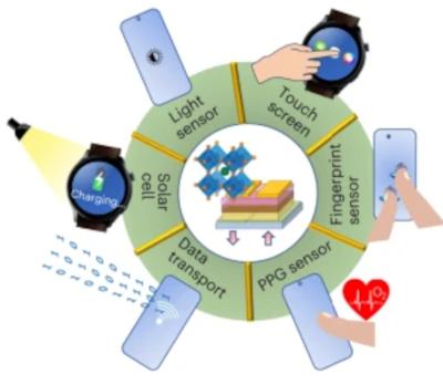
Researchers at Linköping University, Nanjing University and NanjingTech have developed a multifunctional display that uses photo-responsive metal halide perovskite LEDs as pixels. The perovskite LED display can be simultaneously used as a touch screen, ambient light sensor and image sensor (including for fingerprint drawing) without integrating any additional sensors. The light-to-electricity conversion efficiency of the pixels also allow the display to act as a photovoltaic device that can charge the equipment.

Illustration of functions realized by the multifunctional display. Image from Nature Electronics

This is a step forward compared to current display screens, which are typically only used for information display, but can have a range of different sensors integrated into them for functions such as touch control, ambient light sensing and fingerprint sensing. According to the team, photo-responsive light-emitting diodes (LEDs), which can display information and respond to light excitation, could be used to develop future ultra-thin and large screen-to-body ratio screens. However, photo-response is difficult to achieve with conventional display technologies. 

Read the full story Posted: Apr 12,2024