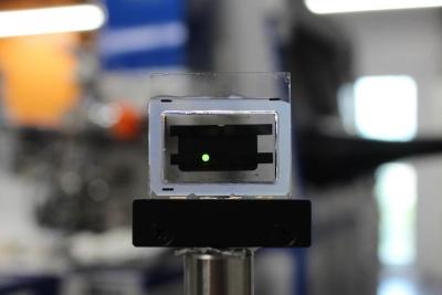
Scientists at Kyushu University in Japan have created micrometer-thick organic light-emitting diodes (OLEDs) by integrating thick layers of hybrid perovskite with thin organic layers. Such devices have the potential to enhance the viewing angles and affordability of high-performance TVs and various other displays.
 A test organic light-emitting diode (OLED) incorporating thick layers of hybrid perovskite emits green light. (Image credit: William J. Potscavage Jr., Kyushu University)
OLEDs use layers of organic molecules to efficiently change electricity into light. While these molecules are excellent emitters, they are usually poor conductors of electricity. This is why researchers strive to use extremely thin layers (around 100 nm) to allow electricity to easily reach where emission takes place in the center of the devices.
As a result, it has been difficult to develop thicker devices and at the same time prevent disadvantageous effects. In order to do so, Kyushu University researchers used specific perovskites that are transparent while also being highly conductive.
Toshinori Matsushima, Study Lead Researcher and Associate Professor, International Institute for Carbon-Neutral Energy Research, Kyushu University, said: '...perovskites based on a blend of organic and inorganic components can be processed from low-cost starting materials using the same fabrication processes as for organics, making perovskites and organics a perfect match.'
The scientists closely packed an emitting layer of molecules within their devices. These molecules are often utilized in OLEDs between perovskite layers that have an overall thickness of 2,000 nm. The devices, thus obtained, possess active layers that are as much as 10-fold thicker than standard OLED devices'although still a fraction of the thickness of a human hair.
The efficiencies of these thick devices were analogous to those found in reference thin OLEDs. In addition, these devices have the same color from each viewing angle. By contrast, OLEDs predicated on thick organic layers did not produce any light at analogous operating voltages.
'These results overturn 30 years of thinking that OLEDs are limited to thin films and open new paths for low-cost, reliable, and uniform fabrication of OLED-based displays and lighting,' stated Professor Chihaya Adachi, director of the Center for Organic Photonics and Electronics Research at Kyushu University.
Scientists have also been trying to apply perovskites directly as light emitters, but to date, the lifespans of these devices have been very short.
By maintaining the emission process in the organic materials and utilizing perovskites simply for transmitting electricity, the Kyushu University research team accomplished comparable lifetimes for both reference OLEDs and thick devices.
'Based on this work, perovskites will be seen in a new light as versatile, high-performance materials for supporting roles in not only OLEDs but also other organic electronic devices, such as lasers, memory devices, and sensors,' predicted Adachi.
Comments
Reference
Reference: https://www.nature.com/articles/s41586-019-1435-5