Perovskites are materials that share a crystal structure similar to the mineral called perovskite, which consists of calcium titanium oxide (CaTiO3).
Depending on which atoms/molecules are used in the structure, perovskites can possess an impressive array of interesting properties including superconductivity, ferroelectricity, charge ordering, spin dependent transport and much more. Perovskites therefore hold exciting opportunities for physicists, chemists and material scientists.
Graphene is a one-atom-thick layer of carbon atoms arranged in a hexagonal lattice. It is the building-block of Graphite (which is used, among others things, in pencil tips), but graphene is a remarkable substance on its own - with a multitude of astonishing properties which repeatedly earn it the title “wonder material”. Graphene is the thinnest material known to man at one atom thick, and also incredibly strong - about 200 times stronger than steel. On top of that, graphene is an excellent conductor of heat and electricity and has interesting light absorption abilities. These varied properties make it a promising and highly researched material, with hopes of incorporating it in many applications: from inks and composite materials, through sensors, solar cells and water filters, to batteries and supercapacitors.
Due to their unique properties, carbon-based nanomaterials have been the center of extensive research efforts in various fields, one of which is the field of photovoltaic energy conversion. In recent years, hybrid metalorganic halide perovskites have become one of the most promising materials for third generation solar cells, with efficiencies that are constantly on the rise.
The incorporation of graphene into perovskite-based solar cells was naturally proposed, and significant work is taking place on this matter. Graphene-based perovskite solar cells are studied in many ways, including hole and electron transport media (HTM and ETM), electrodes, and various approaches aiming at improving the stability of the device. Tandem architectures based on graphene interlayers are also of great interest.
In addition to solar cells, other areas of graphene and perovskite integration include sensors and photodetectors, QDs, nanocatalysts and more.
The latest Perovskite Graphene news:
Graphene Flagship's GRAPES project to promote graphene-enabled perovskite solar panels
The Graphene Flagship, a $1 billion European graphene initiative, has launched a new Spearhead Project called GRAPES, that aims to make cost-effective, stable graphene-enabled perovskite solar panels.
The project will set out to play an essential role in improving Europe's uptake of solar energy projects by improving the stability and efficiency of this technology when deployed on a large scale. As a European Commission funded project, the Graphene Flagship GRAPES initiative has been established to help Europe meet its ambitious sustainability goals.
A new method overcomes the drawback of perovskite grain boundaries by using 2D materials for conducting hole currents
A team of scientists, led by Professor Feng Yan from Department of Applied Physics, The Hong Kong Polytechnic University, Hung Hom, Kowloon, Hong Kong, and co-workers, recentky developed a novel method to overcome the drawback of grain boundaries (GBs) in perovskites without using defect passivation.
Several 2D materials, including black phosphorus (BP), MoS2 and graphene oxide (GO), were specifically modified on the edge of perovskite GBs by a solution process. The 2D materials have high carrier mobilities, ultrathin thicknesses and smooth surfaces without dangling bonds. The PCEs of the devices are substantially enhanced by the 2D flakes, in which BP flakes can induce the highest relative enhancement of about 15%.
Researchers reach excellent results on air processed methylammonium free PSCs via scalable technique
A research team, led by Dr. Luigi Angelo Castriotta at the at University of Rome Tor Vergata's CHOSE Center for Hybrid and Organic Solar Energy, has reported impressive results on methylammonium free perovskites processed in air, using a scalable technique based on infrared annealing and potassium doped graphene oxide as an interlayer.
The team reached efficiencies of 18.3% and 16.10% on 0.1cm2 cell and on 16cm2 module respectively, with enhanced stability compares to the standard multi cation reference.
Researchers design novel X-ray photodetectors based on perovskites on top of graphene
A team of scientists, led by László Forró from the School of Basic Sciences at the Ecole Polytechnique Federale de Lausanne (EPFL) in Switzerland, has developed a new X-Ray Photodetector based on perovskites and graphene.
Using 3D aerosol jet-printing technology, the team designed a new technique for creating highly efficient x-ray photodetectors that can be easily added to standard microelectronic circuits, creating more powerful medical imaging devices that can deliver better scan qualities.
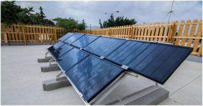
Graphene-perovskite solar farm trial up and running in Greece
An experimental graphene-based perovskite solar farm has been operating in Greece for several months, and early results are said to be very promising when it comes to power output and efficiency.

Located at the Hellenic Mediterranean University in Crete and spearheaded by the EU's Graphene Flagship, the new solar farm consists of nine graphene'perovskite panels with a total area of 4.5m2 and a total output of approximately 261 watt-peak (Wp).
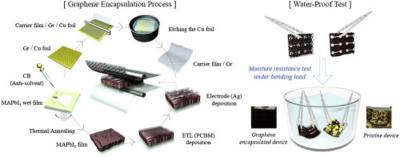
Novel graphene-based encapsulation opens door to robust perovskite solar cells
Researchers at Pusan National University, Gwangju Institute of Science and Technology and the Korea Institute of Machinery & Materials (KIMM) in South Korea have tackled perovskite solar cells' stability issues by designing a graphene-based encapsulation technique.

The team introduced a highly flexible and stable graphene encapsulant by adopting the dry transfer method based on a roll-based process.
Graphene boosts perovskite single crystal photodetector performance
The performance of photodetectors based on perovskite polycrystalline thin films is still considered to be at a distance from expected values. One reason is that the carrier transport at the interface is easily affected by grain boundaries and grain defects. Many research groups have tried to combine perovskite polycrystalline thin films with high-mobility, two-dimensional materials to improve device performance, and have achieved promising results, but the negative effects of perovskite polycrystalline grain boundaries still remain.
To solve this problem, a team led by Assoc. Prof. Yu Weili from Changchun Institute of Optics, Fine Mechanics and Physics (CIOMP) of the Chinese Academy of Sciences, and Prof. GUO Chunlei from the University of Rochester synthesized a low-surface-defect-density CH3NH3PbBr3 microplate through the inverse temperature crystallization strategy. They prepared an effective vertical structure photodetector combining a high-quality perovskite single crystal with monolayer graphene with high carrier mobility.
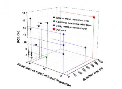
Graphene "shield" improves the stability of perovskite solar cells
A UNIST research team has developed an electrode that can significantly improve the stability of perovskite solar cells. UNIST announced that its research team developed 'flexible and transparent metal electrode-based perovskite solar cells with a graphene interlayer'.

The team suppressed interdiffusion and degradation using a graphene material with high impermeability, the team said. Team leader professor Hyesung Park commented that the research will greatly help not only solar cells but other perovskite-based flexible photoelectric devices such as LEDs and smart sensors.
Perovskite/graphene nanosensor detects nitrogen dioxide with 300% improved sensitivity
A research team led by Juan Casanova and Eduard Llobet from the Departamento de IngenierÃa Electrónica, Eléctrica y Automática at the Universitat Politècnica de València (URV), used graphene and perovskites to create a nanosensor that detects nitrogen dioxide with 300% improved sensitivity.
The team used graphene that is hydrophobic (water and moisture-resistant) and sensitive in gas detection, but with some limitations: it is not very selective and its sensitivity declines over time. In addition, the researchers used perovskites, a crystalline-structure material commonly used in the field of solar cells. However, they quickly deteriorate when they are exposed to the atmosphere. That's the reason why the team decided to combine perovskites with a hydrophobic material able to repel water molecules - in order to prove they can prevent or slow down their deterioration.
Italian research team develops graphene-enhanced tandem perovskite cell with 26.3% efficiency
Italian researchers from two Italian institutions claim to have developed a two-terminal tandem perovskite-silicon solar cell with a conversion efficiency 26.3%.
The researchers added graphene to the titanium dioxide electron selective layer used in a perovskite solar cell to increase chemical stability. The two-terminal cell was made by stacking two sub-cells which were fabricated and optimized separately. The new device blends the advantages of thin-film perovskite and silicon-based heterojunction cells, according to its developers.
Pagination
- Previous page
- Page 2
- Next page

