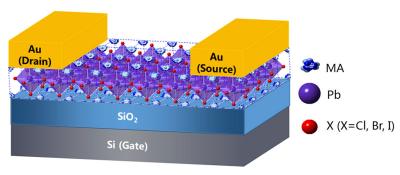
An international team of researchers, led by Aram Amassian at North Carolina State University, has demonstrated the construction of field-effect transistors using a single crystal, hybrid perovskite semiconductor.

While the design of perovskite solar cells has matured to the point of near-commercialization, making hybrid perovskites function as field-effect transistors has been more of a challenge. This is in part due to the fact that perovskite films typically consist of multiple crystals with random orientations that include grain boundaries and various kinds of defects in their atomic crystal lattices. These often limit how well charge carriers (electrons or 'holes') can move through them.
There are techniques that allow perovskite single crystals to be formed, but those crystals typically end up with defects on their surfaces, which makes it difficult to add the necessary electrical contacts. Amassian and his colleagues addressed that problem by fabricating a 2.5-micrometer-thick single perovskite crystal from a solution injected between two flat surfaces separated by a thin spacer'creating a perovskite 'sandwich' of sorts.
The top surface included two gold electrical contacts, which functioned as the transistor's source and drain. The bottom one in this experimental prototype, made of silicon covered by silicon dioxide, served as the transistor's gate and gate insulator.
The FET created by Amassian's team still relies on a silicon substrate. But Amassian explains that they used silicon just to make their pioneering work a bit easier: Other materials, including glass or plastics, for example, could also be used.
The transistors they created in this way required 5 to 10 volts to be applied to the gate to fully turn on, more than any respectable field-effect transistor would need. That's not fundamental to the perovskite material used, though; it's just a function of the rather crude geometry of the early experimental units, Amassian explains.
There's still a long way to go before useful commercial devices of this type can be fabricated, but this work makes a significant step in that direction.

