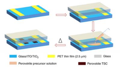
An international team of researchers, including ones from KAUST, the Guo China-US Photonics Laboratory, the University of Rochester and the University of New South Wales, has developed a technique that allows single-crystal hybrid perovskite materials to be integrated into electronics. The team stated that this achievement opens the door to new research into flexible electronics and potentially reduced manufacturing costs for electronic devices.

Challenges in integrating single-crystal hybrid perovskites into electronic devices, such as transistors, have spurred much research focus. The main challenge in incorporating single-crystal hybrid perovskites into electronics stems from the fact that these macroscopic crystals, when synthesized using conventional techniques, have rough, irregular edges. This makes it difficult to integrate with other materials in such a way that the materials make the high-quality contacts necessary in electronic devices.
The researchers can further fine-tune the electrical properties of the perovskite by selecting different halides for use in the perovskite's chemical structure. The choice of halide determines the bandgap of the material, which affects the color appearance of the resulting semiconductor and leads to transparent and even imperceptible electronic devices when using high-bandgap perovskites.
"We have demonstrated the ability to create working field-effect transistors using single-crystal hybrid perovskite materials fabricated in ambient air," says Aram Amassian, corresponding author of a paper on the work and an associate professor of materials science and engineering at NC State.
"That's of interest because traditional single-crystal materials have to be manufactured in ultra-high vacuum, high-temperature environments, and often require exquisite epitaxial growth," Amassian says. "Hybrid perovskites can be grown from solution, essentially from an ink, in ambient air at temperatures below 100 degrees Celsius. This makes them attractive from a cost and manufacturing standpoint. It also makes them compatible with flexible, plastic-based substrates, meaning that they may have applications in flexible electronics and in the internet of things (IoT)".
"That said, there are still major challenges here," Amassian says. "For example, current hybrid perovskites contain lead, which is toxic and therefore not something that's desirable for applications like wearable electronics. However, research is ongoing to develop hybrid perovskites that don't contain lead or that are even entirely metal-free. This is an exciting area of research, and we feel this work is a significant step forward for the device integration of these materials, leading to the development of new technological applications."

