An international research team develops method for printing nanolasers from perovskites

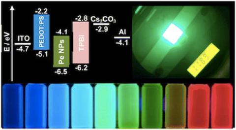
An international research team has developed a new method of synthesizing miniature light sources. The method is based on a unique laser which produces millions of nanolasers from a perovskite film in a few minutes. Such lasers look like small disks, work at room temperature and have a tunable emission wavelength from 550 to 800 nm. The high speed and good reproducibility of this method make it promising for the industrial production of single nanolasers as well as whole chains.

An international research team develops method for printing nanolasers from perovskitesA scheme of the synthesis and operation and an image of the final nanolasers

Such miniature light sources or nanolasers are required, for example, for producing optical chips that could process information in next-gen devices. However, making such light sources is generally not that easy due to unstable materials, as well as the complex and expensive fabrication methods, which are difficult to control and adjust for industrial production. The scientists from ITMO, the Far Eastern Federal University, Texas University at Dallas, and the Australian National University have found a new way to solve this problem. They have developed a method that may enable the creation of millions of nanolasers from an optically active halide perovskites in a few minutes.

Read the full story Posted: Mar 14,2019

Researchers demonstrate controlled epitaxial growth of all inorganic lead-free halide perovskites

A research team composed of scientists from Michigan State University and University of Michigan has deployed a new approach to growing all inorganic lead-free halide perovskites.

Perovskite quantum wells scheme image

"Epitaxial growth has long since revolutionized the study of many electronic materials including silicon, oxide perovskites, and III-V semiconductors," said Richard Lunt, an Associate Professor at Department of Chemical Engineering and Materials Science, Michigan State University who has supervised the project. "There is very little known about the epitaxial growth of halide perovskites, but these exciting materials hold enormous potential. This has motivated us to explore this entirely new research area."

Read the full story Posted: Apr 02,2018

Perovskite-Info interviews Ossila's lead perovskite scientist

UK-based Ossila provides components, equipment and materials to enable faster and smarter organic electronics research and discovery. Ossila provides both materials and equipment for perovskite researchers, and the company's lead perovskite scientist, Dr. Jonathan Griffin, was kind enough to answer a few questions we had for him.

Perovskite crystals (Ossila)Thanks to improved knowledge about salt-solvent interactions, single crystals of perovskites can now be grown. Pictured above are several single-crystal MAPbBr perovskites, alongside the seed crystals used to grow these crystals

Dr. Griffin holds nearly a decade of experience working in organic photovoltaic research and over 5 years of working with perovskites. At Ossila, Jonathan works on technical support for several material ranges, including perovskites, organic photovoltaics, graphene and other 2-D materials. He is also involved in the development of new test equipment and product ranges. Prior to this, he worked in a postdoctoral research position at the University of Sheffield.

Q: Thank you for your time Dr. Griffin. Can you detail for us Ossila's perovskite product range in general?

Read the full story Posted: Mar 08,2018

Unique properties of perovskite materials may lead to better LEDs

Researchers at the U.S. Naval Research Laboratory (NRL) Center for Computational Materials Science, working with an international team of physicists, have found that nanocrystals made of cesium lead halide perovskites (CsPbX3), is the first discovered material which the ground exciton state is "bright," making it an attractive candidate for more efficient solid-state lasers and light emitting diodes (LEDs).

The work focused on lead halide perovskites with three different compositions, including chlorine, bromine, and iodine. Nanocrystals made of these compounds and their alloys can be tuned to emit light at wavelengths that span the entire visible range, while retaining the fast light emission that gives them their superior performance.

Read the full story Posted: Feb 01,2018

Perovskites may bring organic diode lasers one step closer to reality

Researchers from Penn State and Princeton University have made strides in creating a diode laser based on a perovskite material that can be deposited from solution on a laboratory benchtop.

Organic diode lasers, that are extremely hard to make, are sought after since they have many advantages. First, because organic semiconductors are relatively soft and flexible, organic lasers could be incorporated into new form factors not possible for their inorganic counterparts. While inorganic semiconductor lasers are relatively limited in the wavelengths, or colors, of light they emit, an organic laser can produce any wavelength a chemist cares to synthesize in the lab by tailoring the structure of the organic molecules. This tunability could be very useful in applications ranging from medical diagnostics to environmental sensing.

Read the full story Posted: Nov 22,2017

Researchers use lasers to induce alpha state in perovskite materials

Researchers from KU Leuven from the Roeffaers Lab and the Hofkens Group have discovered a new way to create the sought-after dark alpha-phase perovskite. They used direct laser writing (tuned intense laser light) to locally heat the perovskite surface, making it change from the (useless) delta state to the (highly desirable) alpha state.

Lasers can help induce alpha state in perovskites image

Furthermore, they also found that the material now remained in this state for many weeks, even at room temperature, without further need of a stabilizing treatment. The scientists further managed to use the laser beam to rapidly micro-fabricate complex patterns of the dark FAPbI3 state. "These findings are a big step forward in locally tailoring the structural, electrical, and optical properties of an important new class of materials and provides an avenue for making customised optical devices, all on demand".

Read the full story Posted: Oct 09,2017

Perovskites enable discharging multiple, bright colors from one nanowire

Researchers at the Department of Energy's Lawrence Berkeley National Laboratory (Berkeley Lab) have demonstrated that halide perovskites are capable of discharging multiple, bright colors from just one nanowire at resolutions as small as 500 nm. This work could impact the development of new applications in optoelectronics, nanoscopic lasers, photovoltaics and more.

Perovskites discharge multiple colors image

The team used electron beam lithography to fabricate halide perovskite nanowire heterojunctions, the junction of two types of semiconductors. The researchers analyzed cesium lead halide perovskite, and then used a common nanofabrication method integrated with anion exchange chemistry to switch out the halide ions to form cesium lead bromide, cesium lead iodide and cesium lead chloride perovskites. Each difference resulted in a different color discharged.

Read the full story Posted: Jun 28,2017

EPFL team develops new method to stabilize perovskite quantum dots

EPFL researchers have designed a new type of inorganic nanocomposite that makes perovskite quantum dots (nanometer-sized semiconducting materials with unique optical properties) exceptionally stable against exposure to air, sunlight, heat, and water.

EPFL team stabilizes perovskite QDs image

Quantum dots made from perovskites have already been shown to hold potential for solar panels, LEDs and laser technologies. However, perovskite quantum dots have major issues with stability when exposed to air, heat, light, and water. The EPFL team has now succeeded in building perovskite quantum dot films with a technique that helps them overcome these weaknesses.

Read the full story Posted: May 30,2017

2D layered perovskite materials poised to improve optoelectronic devices

Researchers at Los Alamos National Laboratory and their partners are creating innovative 2D layered hybrid perovskites that they say can allow greater freedom in designing and fabricating efficient optoelectronic devices. Industrial and consumer applications could include low cost solar cells, LEDs, laser diodes, detectors, and other nano-optoelectronic devices.

Perovskite edges tuned for optoelectronic performance image

They explain that these materials are layered compounds, or a stack of 2D layers of perovskites with nanometer thickness (like a stack of sheets), and the 2D perovskite layers are separated by thin organic layers. "This work could overturn conventional wisdom on the limitations of device designs based on layered perovskites", the team says.

Read the full story Posted: Mar 14,2017

Perovskite-based colloidal solutions make for efficient LEDs

Researchers at Nanyang Technological University in Singapore have fabricated high-performance green light-emitting diodes based on colloidal organometal perovskite nanoparticles. The devices have a maximum luminous efficiency of 11.49 cd/A, a power efficiency of 7.84 lm/W and an external quantum efficiency of 3.8%. This value is said to be about 3.5 times higher than that of the best colloidal perovskite quantum-dot-based LEDs previously made.

The team developed a simple way to make a series of colloidal (CH3NH3)PbX3 nanoparticles with an amorphous structure that can be tuned to emit light in the ultraviolet to near-infrared range. They studied the photoluminescence properties of the nanoparticles and found that the PLQE of the perovskite NP film is much higher than that of the bulk film. They then made the highly efficient green LED.

Read the full story Posted: Jul 11,2016