Researchers develop high-resolution perovskite nanocrystal patterning technique for displays
Researchers from the Ulsan National Institute of Science and Technology (UNIST) have teamed up with researchers from Daegu Gyeongbuk Institute of Science and Technology (DGIST) to develop a patterning technique for the production of perovskite nanocrystal displays which are ultra-thin and high-resolution. The production involves a very simple stamp-like printing process that will facilitate the commercialization of the new technique.
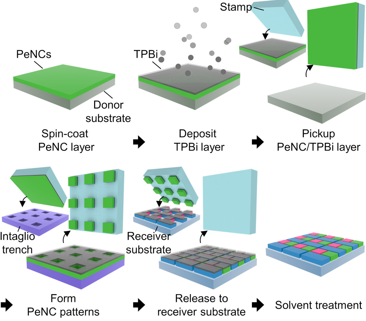
Double-layer transfer printing process with RGB pixelated arrays of PeNCs. Image from Science Advances
The technique reportedly enabled the team to produce a display with RGB pixel patterns of 2,550 pixels per inch, which is about 400 percent higher resolution than the latest high-end smartphones.
Read the full story
Posted: Nov 01,2022