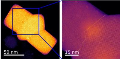
A team of scientists from Washington University in St. Louis, Oak Ridge National Laboratory and University of Missouri studied the structure and properties of the commonly occurring planar defects at the atomic scale of lead halide perovskite.

When these materials are made, defects can occur where different crystals meet, known as grain boundaries. In conventional semiconductors, these defects can decrease their electrical conductivity and the solar energy-to-electricity conversion efficiency; however, in lead-halide perovskites, there are differing experimental reports on the activity of grain boundaries. In some cases, they are found to be harmful, while in other cases they either have no impact on performance or are even beneficial. But, to date, no one understood why. The research team in this work set out to discover these reasons.
At Oak Ridge National Lab, the team members performed the imaging with one of the most powerful electron microscopes to look at the atomic structure of the grain boundaries. They then used quantum-mechanical calculations performed on some of the fastest supercomputers to understand the electronic properties of these grain boundaries.
In silicon semiconductors, grain boundaries usually carry disastrous effects, but in lead-halide perovskites, they may not. And that depends on concentration of the halide ions, a critical element to the properties.
"If you grow the crystals in a halide-poor environment, then the grain boundaries are terrible for performance," the team said. "But if you can grow them or anneal [heat and recombine] them in a halide-rich atmosphere, the grain boundaries are fine."
The team also looked at another type of planar fault known as Ruddlesden-Popper faults, in which the planes of crystals stack incorrectly; for example, instead of being lined up in neat rows, one of the rows is shifted slightly left or right by an atomic column. Again, by using quantum mechanical calculations, it was found that by having a large density of such stacking faults, it might be possible to obtain bright optical emission from large and more stable nanoparticles of certain lead-halide perovskites, which could potentially pave the way for LEDs with longer lifetimes.
"The challenge for experimentalists is to engineer stacking faults at periodic distances," the researchers said.

