Researchers from the Chinese Academy of Sciences (CAS), Anhui University, Ocean University of China and Peking University have reported a one-step space confinement and antisolvent-assisted crystallization (SC-ASC) strategy for large-scale high-quality perovskite single crystal array for optoelectronic device integration.
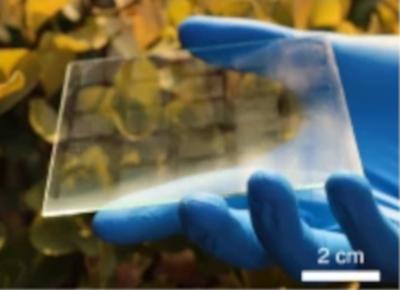
MAPbBr3 MPs array fabricated on the 10 × 10 cm glass
This method provides comprehensive control over the perovskite single crystal array, including the array shape and resolution with crystal dimension and position accuracy as well as the in-plane rotation of the individual single crystal in a large-scale array configuration.
The as-fabricated perovskite single crystal can be served as a high-quality microcavity for WGM laser emission with a high Q factor of 2915 and a low threshold of 4.14 μJ/cm2. Thanks to the regulation of the perovskite array as well as its excellent uniformity, a perovskite photodetector array based on the vertical structure has been demonstrated, showing a stable dynamic photobehavior and imaging capability. This approach for the fully controlled growth of perovskite array combining the conventional photolithography and solution processing procedures of perovskites offers a manufacturing platform for integrated functional photonics and optoelectronics.
The scientists summarize the keys to realizing fully controlled growth of high-quality perovskite arrays: “Substrate engineering defines the array resolution and pixel position, spatial confinement could regulate the extraction of contact lines to ensure that only one crystal is formed in the defined position, and antisolvent-assisted crystallization improves the crystal quality of each pixel.”
“SC-ASC is an effective method for fabricating large-scale single-crystalline perovskite arrays because it incorporates the conventional photolithography process. 25 perovskite arrays have been demonstrated on a 10 × 10 cm glass substrate,” they added.
“Since the readily regulation of the perovskite array as well as its excellent uniformity, the crystal arrays can be directly aligned for integration into large-scale optoelectronic devices. This landmark breakthrough in demonstrating fully controlled on-chip growth of the perovskite single crystal arrays could enable unprecedented applications in vision sensing, light imaging, and large-scale integrated devices,” they predict.


