Perovskites are materials that share a crystal structure similar to the mineral called perovskite, which consists of calcium titanium oxide (CaTiO3).
Depending on which atoms/molecules are used in the structure, perovskites can possess an impressive array of interesting properties including superconductivity, ferroelectricity, charge ordering, spin dependent transport and much more. Perovskites therefore hold exciting opportunities for physicists, chemists and material scientists.
Sensors are devices that detect events that occur in the physical environment (like light, heat, motion, moisture, pressure, and more), and respond with an output, usually an electrical, mechanical or optical signal. The household mercury thermometer is a simple example of a sensor - it detects temperature and reacts with a measurable expansion of liquid. Sensors are everywhere - they can be found in everyday applications like touch-sensitive elevator buttons and lamp dimmer surfaces that respond to touch, but there are also many kinds of sensors that go unnoticed by most - like sensors that are used in medicine, robotics, aerospace and more.
Traditional kinds of sensors include temperature, pressure (thermistors, thermocouples, and more), moisture, flow (electromagnetic, positional displacement and more), movement and proximity (capacitive, photoelectric, ultrasonic and more), though innumerable other versions exist. sensors are divided into two groups: active and passive sensors. Active sensors (such as photoconductive cells or light detection sensors) require a power supply while passive ones (radiometers, film photography) do not.
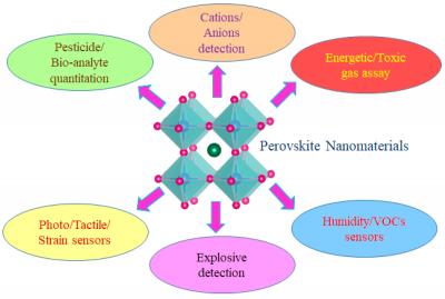
Perovskite materials’ host of exciting properties, such as being rather tolerant to defects (unlike metal chalcogenides) and not requiring surface passivation to retain high quantum yields, make them especially suited for sensing applications. The sensitivity, selectivity, and stability of many perovskite nanomaterials has directed many researchers to devote the most attention to chemical sensors, but perovskites are suitable for other types as well. Perovskites are being studied by numerous research groups for use in various types of sensors.
Researchers develop wearable photoferroelectric perovskite X-Ray detectors
Researchers from China's Shaanxi Normal University, Zhejiang Normal University, China Institute of Radiation Protection and Chinese Academy of Sciences have developed lead-free photoferroelectric hybrid metal halide perovskite flexible membranes for wearable detectors, that offer excellent X-ray response with high sensitivities, low detection limit and impressive imaging capabilities.

Demonstration and application potential for lead-free photoferroelectric perovskite membrane (LFPPM). a) Optical images of the LFPPM. b) Schematic diagram of LFPPM wearable X-ray dosimeter. c) Schematic diagram of the working principle of wearable X-ray dosimeter. (Image credit: Nanowerk)
High-sensitivity wearable radiation detectors are important for personnel protection in radiation environments such as defense, nuclear facilities, and medical fields. Traditional detectors using bulk crystals tend to lack flexibility. Hybrid metal halide perovskites have shown promise for next-generation radiation detection as they can efficiently absorb high-energy radiation and convert it into electrical signals. However, there are concerns of lead toxicity. More recent efforts have explored lead-free alternatives, but these have generally suffered from poor charge transport properties, reducing their effectiveness as radiation detectors.


Researchers develop perovskite-based bird-eye-inspired camera for enhanced object detection
Researchers from Gwangju Institute of Science and Technology (GIST) and Institute for Basic Science (IBS) have developed a perovskite-based camera, inspired by the structures and functions of birds' eyes, specializing in object detection.

Schematic illustration showing the visual ecology of birds. Image from Science Robotics
The eyes of different organisms in the natural world have evolved and been optimized to suit their habitat and the environment in which they survive. As a result of countless years of evolutionary adaptation to the environment of living and flying at high altitudes, bird eyes also have unique structures and visual functions. In the retina of an animal's eye, there is a small pit called the fovea that refracts the light entering the eye. Unlike the shallow foveae found in human eyes, bird eyes have deep central foveae, which refract the incoming light to a large extent. The region of the highest cone density lies within the foveae, allowing the birds to clearly perceive distant objects through magnification. This specialized vision is known as foveated vision.
Empa and ETH researchers are working to improve cameras with perovskite image sensors
Empa and ETH Zurich researchers are working to develop image sensors made of perovskite that could deliver true-color photos even in poor lighting conditions. Unlike conventional image sensors, where the pixels for red, green and blue lie next to each other in a grid, perovskite pixels can be stacked, thus greatly increasing the amount of light each individual pixel can capture.
A consortium comprising Maksym Kovalenko from Empa's Thin Films and Photovoltaics laboratory, Ivan Shorubalko from Empa's Transport at Nanoscale Interfaces laboratory, as well as ETH Zurich researchers Taekwang Jang and Sergii Yakunin, is working on an image sensor made of perovskite capable of capturing considerably more light than its silicon counterpart.
Researchers develop perovskite/organic tandem device for dual light detection and emission functions
Researchers at China's Nanjing University of Science and Technology, Hong Kong Baptist University and Southwest University have introduced a tandem device that incorporates an organic photodiode (OPD) and a perovskite light emitting diode (PeLED), enabling simultaneous light detection and emission in one compact device, prepared by all-solution fabrication process.
The team found that precise control of interfacial properties plays a critical role in establishing the all-solution processed OPD/PeLED multi-layered dual-function device which is critical for charge transport, recombination, and generation.
KEP Technologies develops perovskites-based radiation detection devices
Halide perovskite single crystals such as MAPbBr3 or CsPbBr3 possess properties that make them particularly interesting for the detection of ionizing radiation. The most important of these are their high stopping power for absorbing gamma rays, their low-dark current and effective-charge-transport capability. They are therefore ideal for efficiently producing charges when gamma rays pass through them, which is a basic function required for their use in a detection device.
KEP Technologies, through its Setsafe brand, is developing prototype-level radiation detection devices that incorporate halide perovskite single crystals and that can trigger an alarm based on various criteria. These devices target applications for defense and public protection against nuclear and radiological risks.
Macnica develops a new air quality sensor that uses perovskite solar cells and semi-solid batteries
Macnica, a Technology Solutions Partner that provides products, services, and solutions, has announced a new type of air quality sensor that uses perovskite solar cells and semi-solid batteries. The sensor uses perovskite solar cells from EneCoat Technologies, a startup from Kyoto University.
It was reported that for several years, an indoor perovskite solar cell effectiveness demonstration project has been taking place in the company's office in Tokyo. Through this demonstration project, it was reportedly demonstrated that the technology can become a sustainable energy source in the future, including use under low illumination, and data on various issues was gathered toward the practical application of perovskite solar cells.
Researchers develop perovskite-based synapses for neuromorphic vision sensors
Much research work is put into emulating the human vision system, that can effortlessly and efficiently interpret the visual world despite the barrage of fragmented data that strikes the retina. Neuromorphic visual sensors (NVS) based on photonic synapses hold great promise towards that end, but current photonic synapses rely on delicate engineering of the complex heterogeneous interface to realize learning and memory functions, resulting in high fabrication costs, reduced reliability, high energy consumption and uncompact architecture, severely limiting the up-scaled manufacture, and on-chip integration.
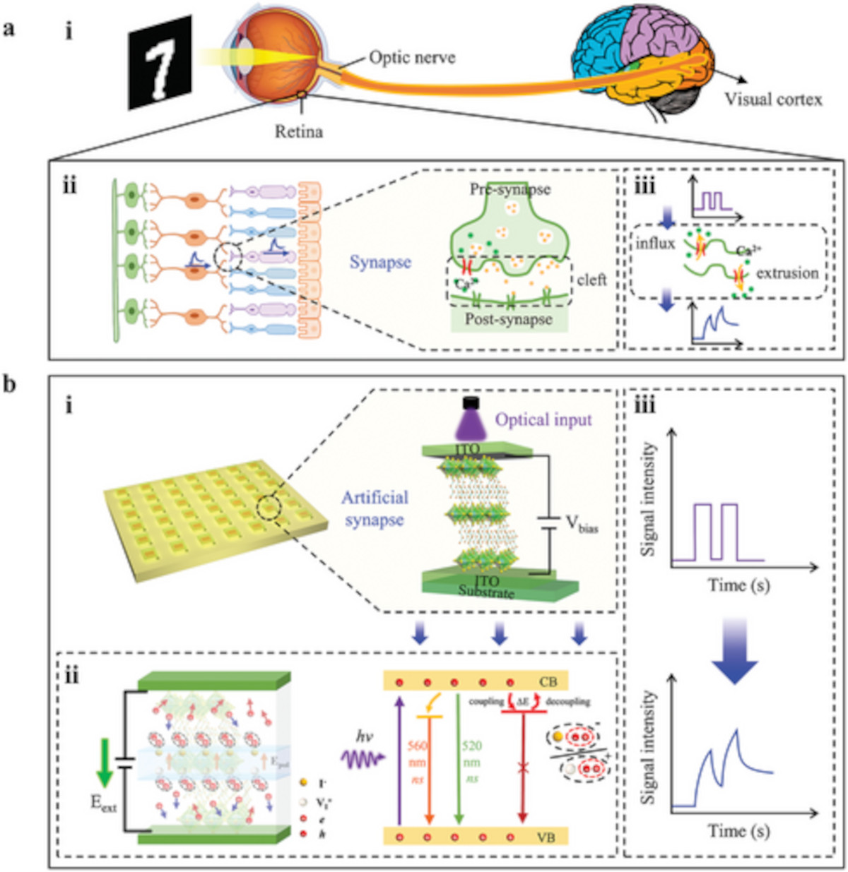
The concept of an artificial visual system mimicking the biological system. a) The biological visual system consisting of the retina (receiving and preprocessing), optic nerves (transmitting), and the visual center (processing and memory system) and a multilayer structure of a retina. b) The artificial visual system based on a 2T vertical photodetector of ITO/(BA)2PbI4/ITO. The exciton-ion coupling is responsible for the nonvolatile photocurrent. Image from Advanced Materials
Now, researchers at Nanjing Normal University, Beijing University of Posts and Telecommunications and RMIT University have reported a nanomaterials-based approach using solution grown hybrid organic-inorganic perovskites (OIHP) that intrinsically unites both photodetection and dynamic, adaptive synaptic signal modulation within single micron scale elements.
Researchers use perovskite films to create lossy mode resonances
Researchers from Spain's Public University of Navarra and Rey Juan Carlos University have used perovskites to create lossy mode resonance (LMR) devices, which are devices that act like super-sensitive detectors that can pick up even the slightest changes in their environment.
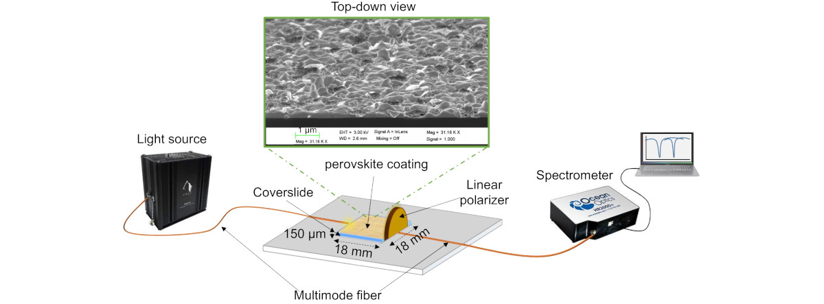
The key to making LMR devices work is choosing the right material for a thin film. Perovskites have unique properties that allow it to generate LMRs, which are like 'sweet spots' where the material interacts with light in a special way. These sweet spots can be fine-tuned by adjusting the thickness of the perovskite film, among other parameters.
Researchers develop perovskite-based humidity sensors integrated with bulk acoustic wave resonators for motion monitoring
Scientists at South China University of Technology and Guangzhou Aifo Communication Technology have develop fast-response humidity sensors based on all-inorganic lead-free Cs2PdBr6 perovskite integrated with bulk acoustic wave resonators for motion monitoring.
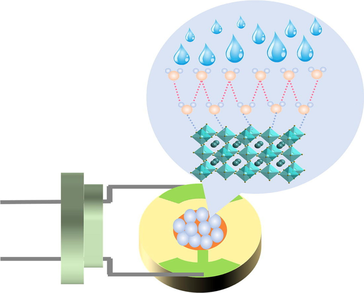
The proposed sensor reportedly exhibits faster response and recovery speed than most other perovskite-based humidity sensors, indicating its potential utilization in real-time monitoring of body movements. In addition, the perovskite-based sensor shows remarkable logarithmic linearity response as well as superior repeatability and stability in the relative humidity range of 11%-85%.
Researchers use perovskite nanocrystals to design bio-inspired imaging sensors capable of “seeing” into the UV range
Researchers at Nanjing University and University of Illinois at Urbana-Champaign have drawn inspiration from the enhanced visual system of the Papilio xuthus butterfly, and developed an imaging sensor capable of “seeing” into the UV range inaccessible to human eyes.
The design of the sensor uses stacked photodiodes and perovskite nanocrystals (PNCs) capable of imaging different wavelengths in the UV range. Using the spectral signatures of biomedical markers, such as amino acids, this new imaging technology is even capable of differentiating between cancer cells and normal cells with 99% confidence.

