Perovskite sensors - Page 2
Researchers use perovskite films to create lossy mode resonances
Researchers from Spain's Public University of Navarra and Rey Juan Carlos University have used perovskites to create lossy mode resonance (LMR) devices, which are devices that act like super-sensitive detectors that can pick up even the slightest changes in their environment.
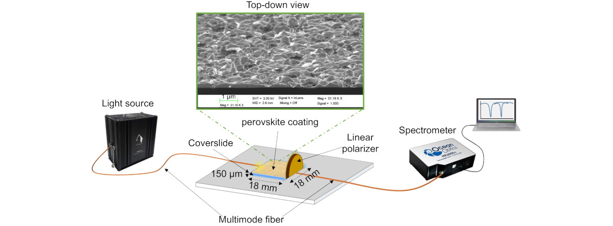
The key to making LMR devices work is choosing the right material for a thin film. Perovskites have unique properties that allow it to generate LMRs, which are like 'sweet spots' where the material interacts with light in a special way. These sweet spots can be fine-tuned by adjusting the thickness of the perovskite film, among other parameters.


Researchers develop perovskite-based humidity sensors integrated with bulk acoustic wave resonators for motion monitoring
Scientists at South China University of Technology and Guangzhou Aifo Communication Technology have develop fast-response humidity sensors based on all-inorganic lead-free Cs2PdBr6 perovskite integrated with bulk acoustic wave resonators for motion monitoring.
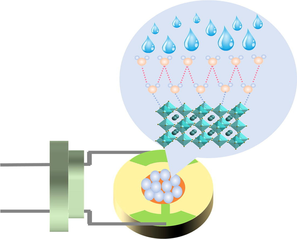
The proposed sensor reportedly exhibits faster response and recovery speed than most other perovskite-based humidity sensors, indicating its potential utilization in real-time monitoring of body movements. In addition, the perovskite-based sensor shows remarkable logarithmic linearity response as well as superior repeatability and stability in the relative humidity range of 11%-85%.
Researchers use perovskite nanocrystals to design bio-inspired imaging sensors capable of “seeing” into the UV range
Researchers at Nanjing University and University of Illinois at Urbana-Champaign have drawn inspiration from the enhanced visual system of the Papilio xuthus butterfly, and developed an imaging sensor capable of “seeing” into the UV range inaccessible to human eyes.
The design of the sensor uses stacked photodiodes and perovskite nanocrystals (PNCs) capable of imaging different wavelengths in the UV range. Using the spectral signatures of biomedical markers, such as amino acids, this new imaging technology is even capable of differentiating between cancer cells and normal cells with 99% confidence.
Researchers examine a perovskite-graphene device for X-ray detection
Researchers at Graphenea, University of Utah and Kairos Sensors have examined a perovskite-based graphene field effect transistor (P-GFET) device for X-ray detection.
The device architecture consisted of a commercially available GFET-S20 chip, produced by Graphenea, with a layer of methylammonium lead iodide (MAPbI3) perovskite spin coated onto the top of it. This device was exposed to the field of a molybdenum target X-ray tube with beam settings between 20 and 60 kVp (X-ray tube voltage) and 30–300 μA (X-ray tube current). Dose measurements were taken with an ion-chamber and thermo-luminescent dosimeters and used to determine the sensitivity of the device as a function of the X-ray tube voltage and current, as well as source-drain voltage.
Researchers report perovskite nanowires-based graphene plasmonic waveguides with low loss and low gain threshold
Researchers at China's Huanghe Science and Technology University, Zhengzhou Normal University and Zhongke Weike Technology (Henan) Co., Ltd have designed a perovskite nanowire-based graphene plasmonic waveguide, where the perovskite nanowire is located on the graphene-insulator-metal (GIM) platform. The findings of this work could have potential applications in plasmonic waveguide-based devices, such as lasers, modulators, sensors, etc.
The finite element method was used in order to investigate the impact of the perovskite nanowire radius, graphene layer thickness, Fermi energy level of the graphene, thickness of the low index dielectric layer, and permittivity of dielectric layer on the mode properties. The results indicate that the hybrid mode exhibits very low propagating loss and ultra-high figure of merit.
Researchers develop ballpoint pens that can write perovskite LEDs on diverse substrates
Researchers from Washington University in St. Louis and Florida State University have developed a versatile, scalable and eco-friendly handwriting approach to draw multicolor perovskite light-emitting diodes and perovskite photodetectors on various substrates, including paper, textiles, plastics, elastomers, rubber and three-dimensional objects.
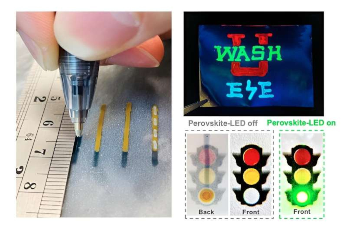
The team's method uses common ballpoint pens filled with newly formulated inks of conductive polymers, metal nanowires and multiple perovskites for a wide range of emission colors. Just like writing with multicolored pens, writing layer-by-layer with these functional inks enables perovskite optoelectronic devices to be realized within minutes.
Researchers develop a platform for integrated spectrometers based on solution-processable semiconductors
Researchers from China's Harbin Institute of Technology and University of Electronic Science and Technology of China have proposed a facile and universal platform to fabricate integrated spectrometers with solution-processable semiconductors by involving the conjugated mode of the bound states in the continuum (conjugated-BIC) photonics.

Acquiring real-time spectral information in point-of-care diagnosis, internet-of-thing, and other lab-on-chip applications requires spectrometers with hetero-integration capability and miniaturized form. Compared to conventional semiconductors integrated by heteroepitaxy, solution-processable semiconductors provide a much-flexible integration platform due to their solution-processability, and, therefore, more suitable for multi-material integrated systems. However, solution-processable semiconductors are usually incompatible with micro-fabrication processes, making them impractical for use in various applications.
Researchers explore how carbon nanotube diameter can influence the performance of photodetector heterojunctions
Researchers from China's Hebei University of Technology and Chinese Academy of Sciences have found that increasing the diameter of single-wall carbon nanotubes (SWCNTs) in SWCNT/perovskite QD heterojunctions can improve the optoelectronic performance of the heterojunction between the two materials.
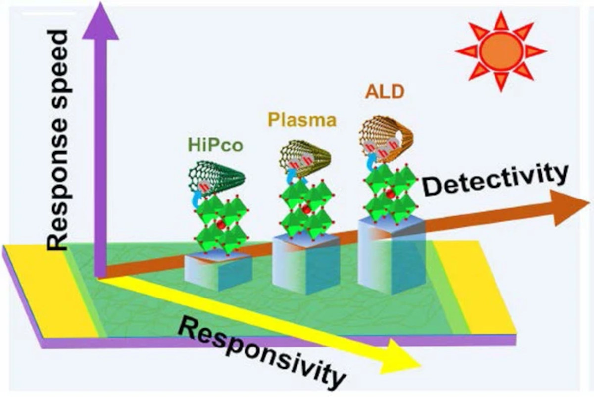
The team systematically tested the performance effects of varying diameters of SWCNTs, a single layer of carbon atoms that form a hexagonal lattice rolled into a seamless cylinder, with different band gaps, or the amount of energy required for an electron to conduct electric current, in heterojunction films with perovskite QDs. Their study indicated that increasing the diameter of SWCNTs improved the responsivity, detectivity and response time of this type of heterojunction film. This effect may be mediated by the enhanced separation and transport of photogenerated excitons, an energy-carrying, neutrally charged electron that combines with a positive electron hole, in the film.
Researchers develop high-performance UV light detector using layered perovskites and textured silicon heterojunction
Researchers from the Zhengzhou University of Light Industry have developed a UV detector of (BA)2PbCl4/textured silicon (BA = n-butylammonium) heterojunction by depositing (BA)2PbCl4 thin film on textured silicon.
High performances of a rapid UV light response (trise = tfall = 0.24 s), high responsivity (8.16 mA/W), and a low detection limit (7.5 μW/cm2) were reportedly obtained from the designed detector, which were ascribed the unique morphology and structure of the detector.
Researchers use perovskites to design LEDs that reveal rot in food before it is visible
Researchers at the Indian Institute of Science Education and Research (IISER) have developed new LEDs which emit light simultaneously in two different wavelength ranges, for a simpler and more comprehensive way to monitor the freshness of fruit and vegetables.
The team explains that modifying the LEDs with perovskite materials causes them to emit in both the near-infrared range and the visible range, a significant development in the contact-free monitoring of food. Angshuman Nag and his team at the Indian Institute of Science Education and Research (IISER) are proposing a perovskite application in LED technology that could simplify the quality control of fresh fruit and vegetables.

