Perovskites are materials that share a crystal structure similar to the mineral called perovskite, which consists of calcium titanium oxide (CaTiO3).
Depending on which atoms/molecules are used in the structure, perovskites can possess an impressive array of interesting properties including superconductivity, ferroelectricity, charge ordering, spin dependent transport and much more. Perovskites therefore hold exciting opportunities for physicists, chemists and material scientists.
Lasers are devices that stimulate atoms or molecules to emit light at particular wavelengths and amplify that light, typically producing a very narrow beam of radiation. The emission usually focuses on an extremely limited range of visible, infrared, or ultraviolet wavelengths.Laser is an acronym for “light amplification by the stimulated emission of radiation”. Lasers are used in extremely diverse industries and applications, like optical disk drives, laser printers, barcode scanners, DNA sequencing instruments, fiber-optics, laser surgery and other medical applications, military and law enforcement devices and much more.
As direct bandgap semiconductors, perovskites exhibit the unique optical properties of bandgap tunability, charge-carrier mobility, defect tolerance, photoluminescence quantum efficiency and power conversion efficiency. These properties make them promising light-emitting materials for high optical gain, low-threshold and multicolor laser applications. The fact that they can be fabricated from low-cost precursors via simple processes makes them attractive as well.
Lower dimensionality perovskite materials, like nanoplatelets, dots, disks, wires etc., can be tailored to be highly desirable for controlled lasing because of their optical cavities and feedback architectures.
Despite their promising features, there are several challenges, for example low exciton binding energy, environmental stability, and formation of trap states at the vicinity of grain interfaces, that need to be addressed when considering perovskite use in lasers. In that respect, 2D perovskites and triple/mixed cation perovskites appear to have potential.


Perovskite-Info launches a new edition of its Perovskite for Displays Market Report
Perovskite-Info is proud to announce an update to our Perovskite for the Display Industry Market Report. This market report, brought to you by the world's leading perovskite and OLED industry experts, is a comprehensive guide to next-generation perovskite-based solutions for the display industry that enable efficient, low cost and high-quality display devices. The report is now updated to July 2024, with all the latest commercial and research activity - including 9 new research papers, new company, new brochures, and commercial updates and more!
Reading this report, you'll learn all about:
- Perovskite materials and their properties
- Perovskite applications in the display industry
- Perovskite QDs for color conversion
- Prominent perovskite display related research activities
The report also provides a list of perovskite display companies, datasheets and brochures of pQD film solutions, an introduction to perovskite materials and processes, an introduction to emerging display technologies and more.


Perovskite-Info launches a new edition of its Perovskite for Displays Market Report
Perovskite-Info is proud to announce an update to our Perovskite for the Display Industry Market Report. This market report, brought to you by the world's leading perovskite and OLED industry experts, is a comprehensive guide to next-generation perovskite-based solutions for the display industry that enable efficient, low cost and high-quality display devices. The report is now updated to February 2024, with all the latest commercial and research activity. This was a major version, with over 15 updates, new companies and new technologies covered.
Reading this report, you'll learn all about:
- Perovskite materials and their properties
- Perovskite applications in the display industry
- Perovskite QDs for color conversion
- Prominent perovskite display related research activities
The report also provides a list of perovskite display companies, datasheets and brochures of pQD film solutions, an introduction to perovskite materials and processes, an introduction to emerging display technologies and more.
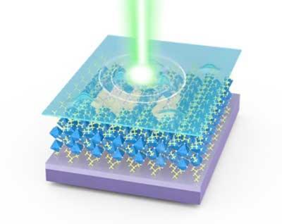
Researchers boost signal amplification in perovskite nanosheets
Researchers at Pusan National University and the University of Oxford have made an advanced in the field of perovskite nanosheets as promising new laser materials. The team overcame the inherent limitations of CsPbBr quantum dots using perovskite nanosheets, which provide enhanced light amplification abilities.
The researchers introduced an innovative waveguide pattern, which increased the gain and thermal stability of the perovskite nanosheets. This pattern improved the optical confinement and heat dissipation, offering a solution to the limitations previously faced with quantum dots. The research team also pioneered a new ‘gain analysis’ method known as the ‘gain contour’. This novel technique provides a more in-depth understanding of gain saturation across various spectrum energies and optical stripe lengths.
Researchers report electrically assisted amplified spontaneous emission in perovskite LEDs
Researchers at Imec have reported a metal halide perovskite LED (PeLED) stack that emits 1,000x more light “than state-of-the-art OLEDs”. The team developed a transparent PeLED architecture, that combines low optical losses with excellent current-injection properties.
In this work, the team showed that perovskite semiconductor optical amplifiers and injection lasers are within reach using this type of transparent PeLED.
Researchers report perovskite nanowires-based graphene plasmonic waveguides with low loss and low gain threshold
Researchers at China's Huanghe Science and Technology University, Zhengzhou Normal University and Zhongke Weike Technology (Henan) Co., Ltd have designed a perovskite nanowire-based graphene plasmonic waveguide, where the perovskite nanowire is located on the graphene-insulator-metal (GIM) platform. The findings of this work could have potential applications in plasmonic waveguide-based devices, such as lasers, modulators, sensors, etc.
The finite element method was used in order to investigate the impact of the perovskite nanowire radius, graphene layer thickness, Fermi energy level of the graphene, thickness of the low index dielectric layer, and permittivity of dielectric layer on the mode properties. The results indicate that the hybrid mode exhibits very low propagating loss and ultra-high figure of merit.
Researchers develop phase-pure 2D tin halide perovskite thin flakes for stable lasing
Researchers from China's Westlake University, Zhejiang University, Binzhou University and U.S-based Purdue University have reported the synthesis of a series of 2D tin perovskite bulk crystals with high phase purity via a mixed-solvent strategy.
Ruddlesden-Popper tin halide perovskites are a class of two-dimensional (2D) semiconductors with exceptional optoelectronic properties, high carrier mobility, and low toxicity. However, the team aimed to address the issue of their challenging synthesis and the lack of fundamental understanding of their optoelectronic properties (compared to their lead counterparts).
Perovskite-Info launches a new edition of its Perovskite for Displays Market Report
Perovskite-Info is proud to announce an update to our Perovskite for the Display Industry Market Report. This market report, brought to you by the world's leading perovskite and OLED industry experts, is a comprehensive guide to next-generation perovskite-based solutions for the display industry that enable efficient, low cost and high-quality display devices. The report is now updated to May 2023, with all the latest commercial and research activity.
Reading this report, you'll learn all about:
- Perovskite materials and their properties
- Perovskite applications in the display industry
- Perovskite QDs for color conversion
- Prominent perovskite display related research activities
The report also provides a list of perovskite display companies, datasheets and brochures of pQD film solutions, an introduction to perovskite materials and processes, an introduction to emerging display technologies and more.
The Perovskite for Displays Market Report updated to September 2022
Perovskite-Info is proud to announce an update to our Perovskite for the Display Industry Market Report. This market report, brought to you by the world's leading perovskite and OLED industry experts, is a comprehensive guide to next-generation perovskite-based solutions for the display industry that enable efficient, low cost and high-quality display devices. The report is now updated to September 2022, with all the latest commercial and research activity.
Reading this report, you'll learn all about:
- Perovskite materials and their properties
- Perovskite applications in the display industry
- Perovskite QDs for color conversion
- Prominent perovskite display related research activities
The report also provides a list of perovskite display companies, datasheets and brochures of pQD film solutions, an introduction to perovskite materials and processes, an introduction to emerging display technologies and more.
Applications of perovskite materials in the display industry
This article was extracted from the Perovskite for Displays market report.
Given perovskites materials' unique optical properties, these materials are being intensively researched for both photovoltaic and display applications (as well as several others). In this article we will take a look into the possible application areas in the display industry that can benefit from perovskite materials.
Perovskite QDs
Perovskite-based QDs (PerQDs) are considered a viable Cd-free alternative for display applications, with high PL quantum yields, wide wavelength tunability and ultra-narrow band emission. The main advantages of PerQDs are:
- Low cost
- High performance
- RoHS compliance (despite the lead content)
The Perovskite for Displays Market Report updated to April 2022
Perovskite-Info is proud to announce an update to our Perovskite for the Display Industry Market Report. This market report, brought to you by the world's leading perovskite and OLED industry experts, is a comprehensive guide to next-generation perovskite-based solutions for the display industry that enable efficient, low cost and high-quality display devices. The report is now updated to April 2022.
Reading this report, you'll learn all about:
- Perovskite materials and their properties
- Perovskite applications in the display industry
- Perovskite QDs for color conversion
- Prominent perovskite display related research activities
The report also provides a list of perovskite display companies, datasheets and brochures of pQD film solutions, an introduction to perovskite materials and processes, an introduction to emerging display technologies and more.

