What are perovskites?
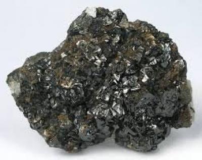
Perovskite is a calcium titanium oxide mineral, with the chemical formula CaTiO3, discovered in the Ural Mountains of Russia by Gustav Rose in 1839 and named after Russian mineralogist Lev Perovski (1792–1856).
Perovskites are a class of materials with a similar structure that are easily synthesized and relatively low-cost. Perovskites are considered the future of solar cells and are also predicted to play a significant role in next-gen electric vehicle batteries, displays, sensors, lasers and much more.
Perovskites can have an impressive collection of interesting properties including “colossal magnetoresistance” - their electrical resistance changes when they are put in a magnetic field (which can be useful for microelectronics). Some Perovskites are superconductors, which means they can conduct electricity with no resistance at all. Perovskite materials exhibit many other interesting and intriguing properties. Ferroelectricity, charge ordering, spin dependent transport, high thermopower and the interplay of structural, magnetic and transport properties are commonly observed features in this family. Perovskites therefore hold exciting opportunities for physicists, chemists and material scientists.
What are LEDs?
A light-emitting diode (LED) is an electronic component that is essentially a two-lead semiconductor light source. It is a p–n junction diode that emits light upon activation by a voltage applied to the leads, which makes electrons recombine with electron holes within the device, releasing energy in the form of photons. This effect is called electroluminescence, and the color of the light is determined by the energy band gap of the chosen semiconductor.
LEDs’ advantages over incandescent light sources include lower energy consumption, longer lifetime, improved physical robustness, smaller size, and faster switching. Light-emitting diodes have become ubiquitous and are found in diverse applications in the aerospace and automotive industries, as well as in advertising, traffic signals, camera flashes and much more.


LEDs meant for general room lighting currently remain more expensive than fluorescent or incandescent sources of similar output, but are significantly more energy efficient.
What can perovskites do for LEDs?
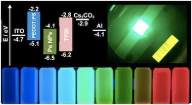
Current high-quality LEDs are based on direct bandgap semiconductors, but making these devices is no easy task because they need to be processed at high temperatures and in vacuum, which makes them rather expensive to produce in large quantities. Perovskites that are direct-bandgap semiconductors could be real alternatives to other types of direct-bandgap materials for applications like color displays, since they are cheap and easy to make and can be easily tuned to emit light of a variety of colors.
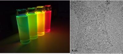
Researchers have found that organometal halide-based perovskites (a combination of lead, organics and halogens that arrange into perovskite crystal structure in the solid state) could be very suitable for making optoelectronics devices, since they can be processed in solution and do not need to be heated to high temperatures. This means that large-area films of these materials can be deposited onto a wide range of flexible or rigid substrates. The perovskites also have an optical bandgap that can be tuned in the visible to infrared regions, which makes them very promising for a range of optoelectronics applications. These materials also emit light very strongly, which makes them very suitable for making LEDs. The light emitted by the perovskites can be easily tuned, which could make them ideal for color displays and lighting, and in optical communication applications.
However, a major obstacle that perovskites will have to overcome in order to be used in LED-type devices is that electrons and holes only weakly bind in perovskite thin films. This means that excitons (electron-hole pairs) spontaneously dissociate into free carriers in the bulk recombination layer, leading to low photoluminescence quantum efficiency (PLQE), high leakage current and low luminous efficiency. This obviously impairs perovskites’ ability to create high-performance LEDs, and for perovskite materials to make a comparable impact in light emission, it is necessary to overcome their slow radiative recombination kinetics. Simply put, researchers will have to find ways of effectively confining electrons and holes in the perovskite so that they can “recombine” to emit light. Major progress is already being made in this field, and it seems that perovskites will indeed open the door to a low-cost, color-tunable approach to LED development.
Recent work in the field of perovskite-based LEDs
In July 2016, researchers at Nanyang Technological University in Singapore have fabricated high-performance green light-emitting diodes based on colloidal organometal perovskite nanoparticles. The devices have a maximum luminous efficiency of 11.49 cd/A, a power efficiency of 7.84 lm/W and an external quantum efficiency of 3.8%. This value is said to be about 3.5 times higher than that of the best colloidal perovskite quantum-dot-based LEDs previously made.
In March 2016, researchers at the University of Toronto in Canada and ShangaiTech University in China have succeeded in using colloidal quantum dots in a high-mobility perovskite matrix to make a near-infrared (NIR) light-emitting diode (LED) with a record electroluminescence power conversion efficiency of nearly 5% for this type of device. The NIR LED could find use in applications such as night vision devices, biomedical imaging, optical communications and computing.
In February 2016, researchers from the Universitat Jaume I and the Universitat de València have studied the interaction of two materials, halide perovskite and quantum dots, revealing significant potential for the development of advanced LEDs and more efficient solar cells. The researchers quantified the "exciplex state" resulting from the coupling of halide perovskites and colloidal quantum dots, both known separately for their optoelectronic properties, but when combined, these materials yield longer wavelengths than can be achieved by either material alone, plus easy tuning properties that together have the potential to introduce important changes in LED and solar technologies.
In December 2015, researchers at Pohang University in Korea are reportedly the first to develop a perovskite light emitting diode (PeLED) that could replace organic LED (OLED) and quantum dot LED (QDLED).
Organic/inorganic hybrid perovskite have much higher color-purity at a lower cost compared to organic emitters and inorganic QD emitters. However, LEDs based on perovskite had previously shown a limited luminous efficiency, mainly due to significant exciton (a complex of an electron and hole that can allow light emission when it is radiatively recombined) dissociation in perovskite layers. The research team overcame the efficiency limitations of PeLED and boosted its efficiency to a level similar to that of phosphorescent OLEDs. This increase was attributed to fine stoichiometric tuning that prevents exciton dissociation, and to nanograin engineering that reduces perovskite grain size, and concomitantly decreases exciton diffusion length. PeLED might be a game changer in the display and solid-state lighting industries, with significantly improved efficiency as well as advantages like excellent color gamut and low material cost.
In November 2015, Florida State researchers have developed a cheaper, more efficient LED, or light-emitting diode, using perovskites. The researchers spent months using synthetic chemistry to fine-tune the materials in the lab, creating a perovskite material capable of emitting a staggering 10,000 candelas per square meter when powered by 12 volts. The scientists say that such exceptional brightness owes, to a large extent, to the inherent high luminescent efficiency of this surface-treated, highly crystalline nanomaterial.
Researchers study interfacial fracture of perovskite light emitting devices
Researchers from the U.S and Ghana recently examined the fracture behavior of Perovskite Light Emitting Devices (PLEDs), emphasizing the importance of interfacial toughness in device performance. This can influence future materials and interface engineering strategies in optoelectronic devices.
Understanding the interfacial fracture toughness of PLEDs can guide the design of more robust devices by improving the adhesion between layers and reducing defect propagation. This can lead to enhanced performance and durability of PLEDs.


Perovskite-Info launches a new edition of its Perovskite for Displays Market Report
Perovskite-Info is proud to announce an update to our Perovskite for the Display Industry Market Report. This market report, brought to you by the world's leading perovskite and OLED industry experts, is a comprehensive guide to next-generation perovskite-based solutions for the display industry that enable efficient, low cost and high-quality display devices. The report is now updated to July 2024, with all the latest commercial and research activity - including 9 new research papers, new company, new brochures, and commercial updates and more!
Reading this report, you'll learn all about:
- Perovskite materials and their properties
- Perovskite applications in the display industry
- Perovskite QDs for color conversion
- Prominent perovskite display related research activities
The report also provides a list of perovskite display companies, datasheets and brochures of pQD film solutions, an introduction to perovskite materials and processes, an introduction to emerging display technologies and more.
Researchers demonstrate spin injection across chiral halide perovskite/III–V interfaces
Researchers from National Renewable Energy Laboratory (NREL), University of Utah, Université de Lorraine CNRS and University of Colorado Boulder have improved upon their previous work, that included incorporating a perovskite layer that allowed the creation of a new type of polarized light-emitting diode (LED) that emits spin-controlled photons at room temperature without the use of magnetic fields or ferromagnetic contacts. In their latest work, they have gone a step further by integrating a III-V semiconductor optoelectronic structure with a chiral halide perovskite semiconductor.
The team transformed an existing commercialized LED into one that also controls the spin of electrons. The results could provide a pathway toward transforming modern optoelectronics, a field that relies on the control of light and encompasses LEDs, solar cells, and telecommunications lasers, among other devices.
Researchers develop second-generation digital display with perovskite LEDs
Researchers from Zhejiang University, LinkZill Technology, Jilin University, and Linköping University have found that the electroluminescence rise time of perovskite LEDs (PeLEDs) can be reduced to microseconds using an individual-particle passivation strategy. This addresses a known issue with PeLEDs, that tend to have electroluminescence rise times over milliseconds due to ion migration in crystal structure, which is problematic for the development of high-refresh-rate displays.
The team demonstrated a second-generation digital display screen that uses perovskite light-emitting diodes instead of standard LED technology. In their study, the group made improvements to the device and demonstrated its sensing capability.
Researchers develop method to create red-emitting perovskite LEDs with record efficiency
Researchers at China's Shanghai University, Jilin University, University of Science and Technology of China, Chinese Academy of Sciences, Korea's Pohang University of Science and Technology (POSTECH) and UK's University of Cambridge have reported efficient and color-stable perovskite LEDs (PeLEDs) across the entire pure-red region, with a peak external quantum efficiency reaching 28.7% at 638 nm, enabled by incorporating a double-end anchored ligand molecule into pure-iodine perovskites.
Light-emitting diodes (LEDs) based on metal halide perovskites (PeLEDs) with high color quality and facile solution processing are promising candidates for full-color and high-definition displays. However, the team explained that despite the great success achieved in green PeLEDs with lead bromide perovskites, it is still challenging to realize pure-red (620–650 nm) LEDs using iodine-based counterparts, as they are constrained by the low intrinsic bandgap.
Researchers design efficient and stable hybrid perovskite-organic LEDs
Researchers at China's Shanghai University, Southern University of Science and Technology, The University of Hong Kong, Yunnan University, Beijing Institute of Technology and Japan's Yamagata University have developed a stable, efficient and high-color purity hybrid light-emitting diodes (LEDs) with a tandem structure, by combining perovskite LED and commercial organic LED technologies.

Device structure. Image credit: Light: Science & Applications
Perovskite-based LED technology can have tunable emission wavelength in visible light range as well as narrow linewidth, which makes it a promising contender among current light-emitting display technologies. However, it still suffers from severe instability driven by electric field. The research team in this work set out to tackle this challenge, by developing a method to create efficient and stable hybrid perovskite-organic light-emitting diodes.
Researchers create full-color fiber light-emitting diodes based on perovskite quantum wires
Researchers from the Hong Kong University of Science and Technology, Sun Yat-sen University and Nanjing University of Science and Technology have uniformly grown all-inorganic perovskite quantum wire arrays by filling high-density alumina nanopores on the surface of Al fibers with a dip-coating process.
Fiber light-emitting diodes (Fi-LEDs), which can be used for wearable lighting and display devices, could be a key component for fiber/textile electronics. However, as a number of challenges exist with this technology, researchers are trying to address issues like on device fabrication with fiber-like substrates, as well as on device encapsulation.
Researchers develop perovskite/organic tandem device for dual light detection and emission functions
Researchers at China's Nanjing University of Science and Technology, Hong Kong Baptist University and Southwest University have introduced a tandem device that incorporates an organic photodiode (OPD) and a perovskite light emitting diode (PeLED), enabling simultaneous light detection and emission in one compact device, prepared by all-solution fabrication process.
The team found that precise control of interfacial properties plays a critical role in establishing the all-solution processed OPD/PeLED multi-layered dual-function device which is critical for charge transport, recombination, and generation.
Researchers develop high-efficiency pure red light-emitting diodes through surface modification of perovskite QDs
Researchers from Korea's Daegu Gyeongbuk Institute of Science and Technology (DGIST), Ulsan National Institute of Science and Technology (UNIST) and Institute for Basic Science (IBS) recently developed high-performance, skin-attachable perovskite pure red light-emitting devices to create various forms of wearable displays.
The team developed these devices through selective surface modification of perovskite quantum dots, expecting their future use in diverse wearable products. As traditional red perovskite materials were unsuitable for high-performance wearable displays due to their low stability and electrical properties, the research team created pure red light-emitting devices through the simple surface modification of the perovskite light-emitting layers, thus significantly improving their stability and electrical properties.
Perovskites’ bright future in the MicroLED industry
Micro-LED (also known as mLED or µLED) is a display technology based on miniature LED devices that are used to directly create color pixels. Micro-LED displays are highly promising and have the potential to create efficient and great looking flexible displays, which could challenge even the most impressive high-end OLED displays. Micro LEDs are attracting significant attention as next-generation displays owing to their desirable characteristics such as low power consumption, high contrast ratio, high brightness, fast response speed, and long life span.

Perovskite materials can benefit the MicroLED industry in two ways: as materials for color conversion (using perovskite-based QDs) and in perovskite-based LED emitters. Much R&D work is taking place on both these fronts, and interest seems to be growing.

