Perovskite LED - Page 2
Researchers demonstrate spin injection across chiral halide perovskite/III–V interfaces
Researchers from National Renewable Energy Laboratory (NREL), University of Utah, Université de Lorraine CNRS and University of Colorado Boulder have improved upon their previous work, that included incorporating a perovskite layer that allowed the creation of a new type of polarized light-emitting diode (LED) that emits spin-controlled photons at room temperature without the use of magnetic fields or ferromagnetic contacts. In their latest work, they have gone a step further by integrating a III-V semiconductor optoelectronic structure with a chiral halide perovskite semiconductor.
The team transformed an existing commercialized LED into one that also controls the spin of electrons. The results could provide a pathway toward transforming modern optoelectronics, a field that relies on the control of light and encompasses LEDs, solar cells, and telecommunications lasers, among other devices.


Researchers develop second-generation digital display with perovskite LEDs
Researchers from Zhejiang University, LinkZill Technology, Jilin University, and Linköping University have found that the electroluminescence rise time of perovskite LEDs (PeLEDs) can be reduced to microseconds using an individual-particle passivation strategy. This addresses a known issue with PeLEDs, that tend to have electroluminescence rise times over milliseconds due to ion migration in crystal structure, which is problematic for the development of high-refresh-rate displays.
The team demonstrated a second-generation digital display screen that uses perovskite light-emitting diodes instead of standard LED technology. In their study, the group made improvements to the device and demonstrated its sensing capability.
Researchers develop method to create red-emitting perovskite LEDs with record efficiency
Researchers at China's Shanghai University, Jilin University, University of Science and Technology of China, Chinese Academy of Sciences, Korea's Pohang University of Science and Technology (POSTECH) and UK's University of Cambridge have reported efficient and color-stable perovskite LEDs (PeLEDs) across the entire pure-red region, with a peak external quantum efficiency reaching 28.7% at 638 nm, enabled by incorporating a double-end anchored ligand molecule into pure-iodine perovskites.
Light-emitting diodes (LEDs) based on metal halide perovskites (PeLEDs) with high color quality and facile solution processing are promising candidates for full-color and high-definition displays. However, the team explained that despite the great success achieved in green PeLEDs with lead bromide perovskites, it is still challenging to realize pure-red (620–650 nm) LEDs using iodine-based counterparts, as they are constrained by the low intrinsic bandgap.
Researchers design efficient and stable hybrid perovskite-organic LEDs
Researchers at China's Shanghai University, Southern University of Science and Technology, The University of Hong Kong, Yunnan University, Beijing Institute of Technology and Japan's Yamagata University have developed a stable, efficient and high-color purity hybrid light-emitting diodes (LEDs) with a tandem structure, by combining perovskite LED and commercial organic LED technologies.

Device structure. Image credit: Light: Science & Applications
Perovskite-based LED technology can have tunable emission wavelength in visible light range as well as narrow linewidth, which makes it a promising contender among current light-emitting display technologies. However, it still suffers from severe instability driven by electric field. The research team in this work set out to tackle this challenge, by developing a method to create efficient and stable hybrid perovskite-organic light-emitting diodes.
Researchers create full-color fiber light-emitting diodes based on perovskite quantum wires
Researchers from the Hong Kong University of Science and Technology, Sun Yat-sen University and Nanjing University of Science and Technology have uniformly grown all-inorganic perovskite quantum wire arrays by filling high-density alumina nanopores on the surface of Al fibers with a dip-coating process.
Fiber light-emitting diodes (Fi-LEDs), which can be used for wearable lighting and display devices, could be a key component for fiber/textile electronics. However, as a number of challenges exist with this technology, researchers are trying to address issues like on device fabrication with fiber-like substrates, as well as on device encapsulation.
Researchers develop perovskite/organic tandem device for dual light detection and emission functions
Researchers at China's Nanjing University of Science and Technology, Hong Kong Baptist University and Southwest University have introduced a tandem device that incorporates an organic photodiode (OPD) and a perovskite light emitting diode (PeLED), enabling simultaneous light detection and emission in one compact device, prepared by all-solution fabrication process.
The team found that precise control of interfacial properties plays a critical role in establishing the all-solution processed OPD/PeLED multi-layered dual-function device which is critical for charge transport, recombination, and generation.
Researchers develop high-efficiency pure red light-emitting diodes through surface modification of perovskite QDs
Researchers from Korea's Daegu Gyeongbuk Institute of Science and Technology (DGIST), Ulsan National Institute of Science and Technology (UNIST) and Institute for Basic Science (IBS) recently developed high-performance, skin-attachable perovskite pure red light-emitting devices to create various forms of wearable displays.
The team developed these devices through selective surface modification of perovskite quantum dots, expecting their future use in diverse wearable products. As traditional red perovskite materials were unsuitable for high-performance wearable displays due to their low stability and electrical properties, the research team created pure red light-emitting devices through the simple surface modification of the perovskite light-emitting layers, thus significantly improving their stability and electrical properties.
Perovskites’ bright future in the MicroLED industry
Micro-LED (also known as mLED or µLED) is a display technology based on miniature LED devices that are used to directly create color pixels. Micro-LED displays are highly promising and have the potential to create efficient and great looking flexible displays, which could challenge even the most impressive high-end OLED displays. Micro LEDs are attracting significant attention as next-generation displays owing to their desirable characteristics such as low power consumption, high contrast ratio, high brightness, fast response speed, and long life span.
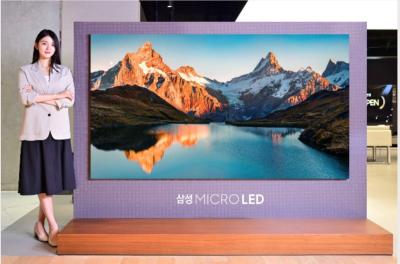
Perovskite materials can benefit the MicroLED industry in two ways: as materials for color conversion (using perovskite-based QDs) and in perovskite-based LED emitters. Much R&D work is taking place on both these fronts, and interest seems to be growing.
Researchers design multifunctional display based on photo-responsive perovskite light-emitting diodes
Researchers at Linköping University, Nanjing University and NanjingTech have developed a multifunctional display that uses photo-responsive metal halide perovskite LEDs as pixels. The perovskite LED display can be simultaneously used as a touch screen, ambient light sensor and image sensor (including for fingerprint drawing) without integrating any additional sensors. The light-to-electricity conversion efficiency of the pixels also allow the display to act as a photovoltaic device that can charge the equipment.
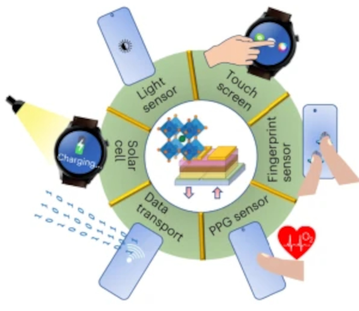
Illustration of functions realized by the multifunctional display. Image from Nature Electronics
This is a step forward compared to current display screens, which are typically only used for information display, but can have a range of different sensors integrated into them for functions such as touch control, ambient light sensing and fingerprint sensing. According to the team, photo-responsive light-emitting diodes (LEDs), which can display information and respond to light excitation, could be used to develop future ultra-thin and large screen-to-body ratio screens. However, photo-response is difficult to achieve with conventional display technologies.
Researchers develop "all-in-one" organic ligand for emitting perovskite nanocrystals
Perovskite nanocrystals (PNCs) have considerable potential as next-generation display materials thanks to their excellent photoluminescence quantum yield (PLQY), wide color gamut, and narrow emission bandwidth. However, due to their weak stability against solvents, their patterning remains a challenge. In a recent study, researchers at Ajou University, Hanyang University, Sungkyunkwan University, Macquarie University and Kongju National University developed functional organic ligands (AzL1-Th and AzL2-Th) for the fine pixelation of perovskite nanocrystal (PNC) displays.
Functional ligands containing photocurable azide moieties exhibit good charge transport properties and fast and efficient photocrosslinking performance, while maintaining a high PLQY. The team successfully demonstrated the crosslinked PNC light emitting diodes using AzL1-Th. The results suggest the high potential of photocurable ligands for the micro-patterning of PNC films without film damages.

