Perovskites are materials that share a crystal structure similar to the mineral called perovskite, which consists of calcium titanium oxide (CaTiO3).
Depending on which atoms/molecules are used in the structure, perovskites can possess an impressive array of interesting properties including superconductivity, ferroelectricity, charge ordering, spin dependent transport and much more. Perovskites therefore hold exciting opportunities for physicists, chemists and material scientists.
Sensors are devices that detect events that occur in the physical environment (like light, heat, motion, moisture, pressure, and more), and respond with an output, usually an electrical, mechanical or optical signal. The household mercury thermometer is a simple example of a sensor - it detects temperature and reacts with a measurable expansion of liquid. Sensors are everywhere - they can be found in everyday applications like touch-sensitive elevator buttons and lamp dimmer surfaces that respond to touch, but there are also many kinds of sensors that go unnoticed by most - like sensors that are used in medicine, robotics, aerospace and more.
Traditional kinds of sensors include temperature, pressure (thermistors, thermocouples, and more), moisture, flow (electromagnetic, positional displacement and more), movement and proximity (capacitive, photoelectric, ultrasonic and more), though innumerable other versions exist. sensors are divided into two groups: active and passive sensors. Active sensors (such as photoconductive cells or light detection sensors) require a power supply while passive ones (radiometers, film photography) do not.
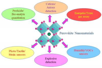
Perovskite materials’ host of exciting properties, such as being rather tolerant to defects (unlike metal chalcogenides) and not requiring surface passivation to retain high quantum yields, make them especially suited for sensing applications. The sensitivity, selectivity, and stability of many perovskite nanomaterials has directed many researchers to devote the most attention to chemical sensors, but perovskites are suitable for other types as well. Perovskites are being studied by numerous research groups for use in various types of sensors.
The latest Perovskite sensor news:
Researchers design spray-coated perovskite hemispherical photodetector
Researchers from China's Jilin University have designed a spray coated spherical perovskite photonic sensor made of phenyl ethyl ammonium/formamidinium lead halide (PEA2FAn-1PbnX3n+1). The researchers utilized the perovskite formulations to regulate the crystallization rate. Cyclic spray-coating and the solution concentration were used to control the coating thickness from a few nanometers to hundreds of micrometers.
Sphere imagers featuring specific wavelength recognition and wide-angle imaging are required in order to meet the fast development pace of modern technology. However, it remains challenging to deposit high-quality photosensitive layers on sphere substrates from low-cost solution processes. In this recent study, the team demonstrated the feasibility of using a rapid spray-coating procedure to fabricate perovskite hemispherical photodetectors that can execute lens-free scanning at nearly 180°, considerably decreasing the reliance on complex optical components.
Researchers develop perovskite-based photodetectors with excellent efficiencies and response times
Researchers at the University of Toronto and the Barcelona Institute of Science and Technology recently reported new solution-processed perovskite photodetectors that exhibit remarkable efficiencies and response times. The photodetectors have a unique design that prevents the formation of defects between its different layers.
The researchers explained that there are applications for which fast photodetection is required in wavelength ranges beyond human vision. "Silicon, the legacy approach—and ideal for electronic readout—does not on its own unite high efficiency with high-speed, as a result of its indirect bandgap, a property of silicon's band structure that produces weak absorption (hence a need for thick silicon) in the near infrared", said University of Toronto's Amin Morteza Najarian.
Researchers design flexible X-Ray detectors based on molecular perovskites
Researchers from China's University of Science and Technology of China (USTC) and Shaanxi Normal University have synthesized a new molecular perovskite, DABCO-CsBr3 (DABCO = N,N′-diazabicyclo[2.2.2]octonium), for use in flexible X-ray detectors. The material was prepared from DABCO, CsBr, and HBr in aqueous solution and obtained in the form of colorless crystals.
The team found that DABCO-CsBr3 possesses good mechanical properties for use in flexible devices. Compared with the metal-free equivalent DABCO-NH4Br3, DABCO-CsBr3 has a stronger X-ray attenuation capability. The researchers built a flexible X-ray detector, using a poly(vinylidene fluoride) (PVDF) polymer matrix that was mixed with DABCO-CsBr3 to create a composite film. This film shows a linear relationship between the X-ray-induced current density and the X-ray dose rate. According to the team, the material could have applications in X-ray security screening systems or medical diagnostics.
Quantum Solutions starts offering evaluation samples of next-gen perovskite-QD based X-Ray Scintillators
UK-based Quantum Solutions started to ship evaluation samples of its next-gen perovskite quantum dots (pQD) X-Ray Scintillators. The company says that these scintillators offer very high sensitivity, high light output, high resolution, low afterglow and can be processed on large areas.
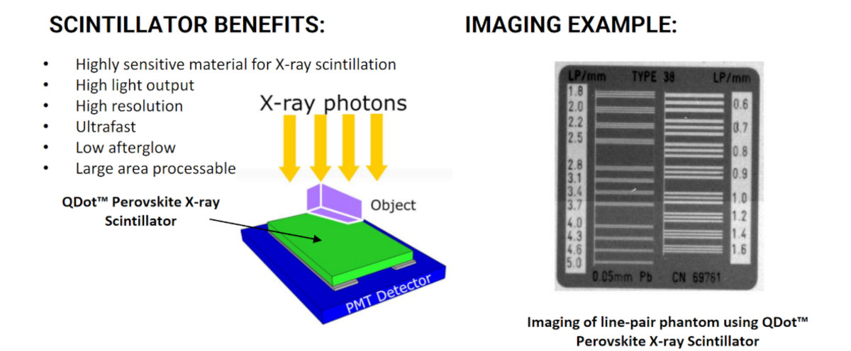
Quantum Solutions started developing these materials in 2020, and already managed to increase the light output (brightness) 10 times over. The company says that this is due to the unique perovskite structure that allows to tune the properties by composition, particle sizes/shapes, ligands, etc. The product already matches the performance of commercial CsI(Tl) and GADOX scintillators. The company is working with key customers in the medical field and non-destructive testing field, and are continuing to develop and customize the product.
Perovskite material for use in high-speed ionizing radiation detectors
Scientists at Russia's NUST MISiS, Moscow Institute of Physics and Technology, the Russian Academy of Sciences, RTU MIREA and Italy's CHOSE (Centre of Hybrid and Organic Solar Energy) have developed a halide perovskite-based material for use in high-speed and highly sensitive ionizing radiation detectors.
Perovskite responds to ionizing radiation in the form of light (luminescence) or current (as a photodiode). This is useful for high-speed and high-sensitivity components for high-energy particle registration. However, the structures inside the collider are exposed to high doses of radiation, which can damage them. Accordingly, components of ionizing radiation detectors must be resistant to such effects and retain their properties for a long time.
Researchers design halide perovskite nanocrystal memristors for neuromorphic computing
Researchers at ETH Zurich, the University of Zurich and Empa have developed a novel concept for a perovskite-based memristor that can be used in a far wider range of applications than existing memristors.
“There are different operation modes for memristors, and it is advantageous to be able to use all these modes depending on an artificial neural network’s architecture,” explains ETH postdoc Rohit John. “But previous conventional memristors had to be configured for one of these modes in advance.” The new memristors can now switch between two operation modes while in use: a mode in which the signal grows weaker over time and dies (volatile mode), and one in which the signal remains constant (non-volatile mode).
Researches show how water can be a positive factor for perovskite crystal growth
Researchers from ARC Centre of Excellence in Exciton Science, Monash University, University of Sydney and CSIRO Manufacturing have shown how water could be the 'secret ingredient' in a simple way to create perovskite crystals.
Ordinarily, water is kept as far away as possible during the process of creating perovskites as the presence of moisture is severely harmful to them. That’s why perovskites for scientific research are often made via spin coating in the sealed environment of a nitrogen glove box. However, in their new work, the researchers have found a simple way to control the growth of phase-pure perovskite crystals by harnessing water as a positive factor. This liquid-based mechanism works at room temperature, so the approach remains cost effective.
An international team secures grant to develop perovskite-based X-ray detectors
A new project, one of eight that successfully secured funding from the Hebrew University of Jerusalem (HUJI) ' Zelman Cowen Academic Initiatives (ZCAI), Australia this year, will focus on developing X-ray detectors from metal halide perovskite materials.
Associate Professor Guohua Jia, from Curtin University's School of Molecular and Life Sciences, said X-ray detectors based on metal halide perovskites are highly sensitive, enabling a very low detection limit, meaning they could lower medical expenses and reduce the risk of radiation to patients.
Researchers develop perovskite-based artificial retina
KAUST researchers have developed an artificial electronic retina based on perovskite materials, that can "see" in a similar way to the human vision system and can recognize handwritten digits.
The team designed and fabricated an array of photoreceptors that detect the intensity of visible light via a change in electrical capacitance, mimicking the behavior of the eye's rod retina cells. When the array was connected to an electronic CMOS-sensing circuit and a spiking neural network (a single-layer network with 100 output neurons), it was able to recognize handwritten numbers with an accuracy of around 70%.
Researchers use inkjet printing to produce a large range of photodetector devices based on a hybrid perovskite semiconductor
Researchers from Innovation Lab HySPRINT at Helmholtz-Zentrum Berlin (HZB) and Humboldt Universität zu Berlin (HU) have used an advanced inkjet printing technique to produce a large range of photodetector devices based on a hybrid perovskite semiconductor.

By mixing three inks, the researchers were able to precisely tune the semiconductor properties during the printing process. Inkjet printing is already an established fabrication method, allowing fast and cheap solution processing. Extending the inkjet capabilities from large area coating towards combinatorial material synthesis could open the door to new possibilities for the fabrication of different kinds of electronic components in a single printing step.

