NUS team harnesses the properties of 2D perovskites for ultrathin optoelectronic applications

NUS scientists have found that the light emission properties of molecularly thin two-dimensional (2-D) hybrid perovskite can be tuned in a highly reversible way for ultrathin optoelectronic applications. A highly efficient photodetector has been fabricated using hybrid perovskites with the thickness of a single quantum well.
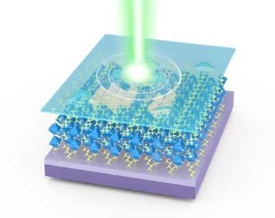
Molecularly thin hybrid perovskite for advanced optoelectronic applications imageAn impression of laser interaction with a molecularly thin 2D perovskites encapsulated by hexagonal boron nitride (blue layer). (Image: NUS)

Each basic unit of a 2D hybrid perovskite is constructed using a semiconducting layer of inorganic material sandwiched between two organic insulating layers. While researchers have studied layered perovskites in their bulk form for many years, the properties of these crystals when their thickness is thinned down to a few and single layers have largely not been explored.
Read the full story Posted: Dec 11,2018

Researchers use novel method to visualize the 3D atomic and electron density structure of the most complex perovskite crystal structure system known to date

A team of researchers from Penn State, Cornell and Argonne National Laboratory have manages to visualize, for the first time, the 3D atomic and electron density structure of the most complex perovskite crystal structure system known to date.

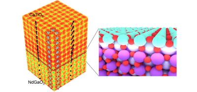
Researchers visualize atomic structure of complex perovskite crystal imageA reconstruction of a perovskite crystal (CaTiO3) grown on a similar perovskite substrate (NdGaO3) showing electron density and oxygen octahedral tilt. Credit: Penn State

The team explains that perovskite crystals have a distinct structure of oxygen atoms that form an octahedron ' an eight-sided polygon. This arrangement of oxygen atoms acts like a cage that can hold a large number of the elemental atoms in the periodic table. Additionally, other atoms can be fixed to the corners of a cube outside of the cage at precise locations to alter the material's properties, for instance in changing a metal into an insulator, or a non-magnet into a ferromagnet.

Read the full story Posted: Dec 11,2018

Researchers develop a polymer film that reduces defects in perovskites

Researchers at the University of California, Los Angeles have used a polymer film to reduce defects in the light-absorbing perovskite, producing solar cells that are efficient and relatively robust.

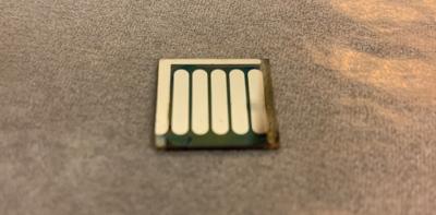
Researchers develop a polymer film that reduces defects in perovskites image

The team explains that perovskites usually used in solar cells typically contain an organic cation and lead halide anions. But the heat treatment used to convert the perovskite's precursors into a crystalline layer can also drive out some of these organic cations. This leaves defects in the material's structure that hamper its performance and potentially make it less stable to moisture, heat, and even sunlight itself.

Read the full story Posted: Dec 03,2018