What are perovskite?
Perovskites are a class of materials that share a similar structure, which display a myriad of exciting properties like superconductivity, magnetoresistance and more. These easily synthesized materials are considered the future of solar cells, as their distinctive structure makes them perfect for enabling low-cost, efficient photovoltaics. They are also predicted to play a role in next-gen electric vehicle batteries, sensors, lasers and much more.

How does the PV market look today?
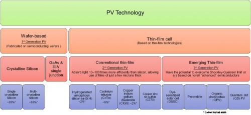
In general, Photovoltaic (PV) technologies can be viewed as divided into two main categories: wafer-based PV (also called 1st generation PVs) and thin-film cell PVs. Traditional crystalline silicon (c-Si) cells (both single crystalline silicon and multi-crystalline silicon) and gallium arsenide (GaAs) cells belong to the wafer-based PVs, with c-Si cells dominating the current PV market (about 90% market share) and GaAs exhibiting the highest efficiency.

Thin-film cells normally absorb light more efficiently than silicon, allowing the use of extremely thin films. Cadmium telluride (CdTe) technology has been successfully commercialized, with more than 20% cell efficiency and 17.5% module efficiency record and such cells currently hold about 5% of the total market. Other commercial thin-film technologies include hydrogenated amorphous silicon (a-Si:H) and copper indium gallium (di)selenide (CIGS) cells, taking approximately 2% market share each today. Copper zinc tin sulphide technology has been under R&D for years and will probably require some time until actual commercialization.
What is a perovskite solar cell?
An emerging thin-film PV class is being formed, also called 3rd generation PVs, which refers to PVs using technologies that have the potential to overcome current efficiency and performance limits or are based on novel materials. This 3rd generation of PVs includes DSSC, organic photovoltaic (OPV), quantum dot (QD) PV and perovskite PV.
A perovskite solar cell is a type of solar cell which includes a perovskite structured compound, most commonly a hybrid organic-inorganic lead or tin halide-based material, as the light-harvesting active layer. Perovskite materials such as methylammonium lead halides are cheap to produce and relatively simple to manufacture. Perovskites possess intrinsic properties like broad absorption spectrum, fast charge separation, long transport distance of electrons and holes, long carrier separation lifetime, and more, that make them very promising materials for solid-state solar cells.

Perovskite solar cells are, without a doubt, the rising star in the field of photovoltaics. They are causing excitement within the solar power industry with their ability to absorb light across almost all visible wavelengths, exceptional power conversion efficiencies already exceeding 20% in the lab, and relative ease of fabrication. Perovskite solar cells still face several challenge, but much work is put into facing them and some companies, are already talking about commercializing them in the near future.
What are the advantages of Perovskite solar cells?
Put simply, perovskite solar cells aim to increase the efficiency and lower the cost of solar energy. Perovskite PVs indeed hold promise for high efficiencies, as well as low potential material & reduced processing costs. A big advantage perovskite PVs have over conventional solar technology is that they can react to various different wavelengths of light, which lets them convert more of the sunlight that reaches them into electricity.
Moreover, they offer flexibility, semi-transparency, tailored form factors, light-weight and more. Naturally, electronics designers and researchers are certain that such characteristics will open up many more applications for solar cells.
What is holding perovskite PVs back?
Despite its great potential, perovskite solar cell technology is still in the early stages of commercialization compared with other mature solar technologies as there are a number of concerns remaining.
One problem is their overall cost (for several reasons, mainly since currently the most common electrode material in perovskite solar cells is gold), and another is that cheaper perovskite solar cells have a short lifespan. Perovskite PVs also deteriorate rapidly in the presence of moisture and the decay products attack metal electrodes. Heavy encapsulation to protect perovskite can add to the cell cost and weight. Scaling up is another issue - reported high efficiency ratings have been achieved using small cells, which is great for lab testing, but too small to be used in an actual solar panel.
A major issue is toxicity - a substance called PbI is one of the breakdown products of perovskite. This is known to be toxic and there are concerns that it may be carcinogenic (although this is still an unproven point). Also, many perovskite cells use lead, a massive pollutant. Researchers are constantly seeking substitutions, and have already made working cells using tin instead. (with efficiency at only 6%, but improvements will surely follow).
What’s next?
While major challenges indeed exist, perovskite solar cells are still touted as the PV technology of the future, and much development work and research are put into making this a reality. Scientists and companies are working towards increasing efficiency and stability, prolonging lifetime and replacing toxic materials with safer ones. Researchers are also looking at the benefits of combining perovskites with other technologies, like silicon for example, to create what is referred to as “tandem cells”.
Commercial activity in the field of perovskite PV
In September 2015, Australia-based organic PV and perovskite solar cell (PSC) developer Dyesol declared a major breakthrough in perovskite stability for solar applications. Dyesol claims to have made a significant breakthrough on small perovskite solar cells, with “meaningful numbers” of 10% efficient strip cells exhibiting less than 10% relative degradation when exposed to continuous light soaking for over 1000 hours. Dyesol was also awarded a $0.5 million grant from the Australian Renewable Energy Agency (ARENA) to commercialize an innovative, very high efficiency perovskite solar cell.
Also in 2015, Saule Technologies signed an investment deal with Hideo Sawada, a Japanese investment company. Saule aims to combine perovskite solar cells with other currently available products, and this investment agreement came only a year after the company was launched.
In October 2020, Saule launched sunbreaker lamellas equipped with perovskite solar cells. The product is planned to soon be marketed across across Europe and potentially go global after that.
In August 2020, reports out of China suggested that a perovskite photovoltaic cell production line has gone into production in Quzhou, east China's Zhejiang Province. The 40-hectare factory was reportedly funded by Microquanta Semiconductor and expected to produce more than 200,000 square meters of photovoltaic glass before the end of 2020.
In September 2020, Oxford PV's Professor Henry Snaith stated that the Company's perovskite-based solar cells are scheduled to go on sale next year, probably by mid 2021. These will be perovskite solar cells integrated with standard silicon solar cells.
Researchers develop stable n–i–p monolithic perovskite/silicon tandem solar cells with over 29% efficiency, based on double-sided poly-Si/SiO2 passivating contact silicon cells
The majority of monolithic perovskite/Si tandem solar cells (TSCs) have been built on heterojunction (HJT) Si solar cells, which have seen limited industrial uptake due to manufacturing cost and concern over the viability of metal electrodes and transparent conductive oxides (TCOs) incorporating expensive elements. Recently, researchers from The Australian National University, University of Melbourne and University of New South Wales demonstrated that high efficiencies of perovskite/Si TSCs can be achieved with Si bottom cells based on a double-side poly-Si/Si dioxide (SiO2) passivating contact (poly-Si cell) without silver or transparent conductive oxides (TCOs), fabricated using mass-production techniques.
In addition, a novel low-absorption, dopant-free bilayer-structured hole transport layer (HTL) composed of ultra-thin poly(N,N′-bis-4-butylphenyl-N,N′-bisphenyl)benzidine (Poly-TPD) and 2,2′,7,7′-tetra(N,N-di-p-tolyl)amino-9,9-spirobifluorene (Spiro-TTB) double layers was developed for the perovskite top cell, which passivates the perovskite surface and enhances the near-interface conductivity, thus increasing the open-circuit voltage and fill factor.
NREL team evaluates sustainability pathways for perovskite photovoltaics
Researchers at NREL have examined how metal halide perovskite photovoltaics (MHP-PV) could scale a sustainable supply chain while appreciably contributing to a global renewable energy transition. They evaluated the critical material concerns, embodied energy, carbon impacts and circular supply chain processes of MHP-PVs.
Perovskite-based solar panels may play an important role amid global decarbonization efforts to reduce greenhouse gas emissions. As the technology emerges from the testing stages, scientists are assessing how best to design the solar panels to minimize their impact on the environment decades from now.
Researchers eliminate grain surface concavities to obtain improved perovskite thin-film interfaces
Researchers at Hong Kong Baptist University, The Hong Kong University of Science and Technology (HKUST) and Yale University have revealed the existence of surface concavities on individual crystal grains that are the fundamental blocks of perovskite thin films, and examined their significant effects on the film properties and reliability.
Based on this discovery, the team designed a new way of making perovskite solar cells (PSCs) more efficient and stable via a chemo-elimination of these grain surface concavities.
First Solar commissions huge solar R&D center
Prominent U.S solar panel maker, First Solar (Nasdaq: FSLR), is reportedly building a new research and development (R&D) innovation center in Lake Township, Ohio, believed to be the largest facility of its kind in the Western Hemisphere - The Jim Nolan Center for Solar Innovation. The new center is part of an approximately half-billion dollar investment by First Solar in R&D infrastructure, and the company expects to also commission a perovskite development line at its Perrysburg, Ohio, campus in the second half of 2024.
The facility covers 1.3 million square feet and includes a high-tech pilot manufacturing line allowing for the production of full-sized prototypes of thin film and tandem PV modules. Prior to the commissioning of the Jim Nolan Center, First Solar utilized a manufacturing line at its Perrysburg facility for its late-stage product development efforts. This arrangement limited the flexibility for development efforts and created constraints when mission-critical tools had to go offline. By resolving these limitations and constraints, the new facility is expected to accelerate innovation cycles.
EneCoat Technologies raises Series C funding of over USD$35 million
INPEX CORPORATION, a large Japanese exploration and production (E&P) company, has announced it has made an investment in EneCoat Technologies, a Kyoto University-based startup company that develops next-generation perovskite solar cells. This is part of a series C round that totaled in 5.5 billion yen (around USD$35 million) and was led by Toyota’s growth fund, Woven Capital and and Mitsubishi HC Capital (in addition to INPEX). Existing investors Mirai Creation Fund III and Kyoto University Innovation Capital participated in the round, bringing the total funding raised to over 8 billion yen (over USD$50 million).
As perovskite solar cells use iodine compounds as raw materials, INPEX is well positioned to tap synergies in terms of raw material supply through its operations at the Naruto Gas Field in Chiba Prefecture, a water-soluble gas field where subsurface brine water is used to produce iodine following the extraction of natural gas.
Researchers examine barrier reinforcement for enhanced perovskite solar cell stability under reverse bias
Researchers at the National Renewable Energy Laboratory (NREL) and University of North Carolina at Chapel Hill have reported a systematic study on the degradation mechanisms of p–i–n structure perovskite solar cells (PSCs) under reverse bias. Reverse bias is a phenomenon that can occur when, for example, an individual cell is shaded and other cells in the module try to push a higher current through it, increasing the temperature and potential damage to the cells. These conditions make solar cells unstable and deteriorate their performance over time.
The team's new strategy could improve the stability of PSCs under reverse bias conditions and facilitate the future deployment of perovskite-based photovoltaics (PVs) in real-world settings.
Singfilm Solar announces 22.6% efficiency for perovskite solar module
Singapore-based startup Singfilm Solar has announced it achieved a power conversion efficiency of 22.6% for a p-i-n structure perovskite solar panel. The result was said to be confirmed by China's National PV Industry Measurement and Testing Center (NPVM).
The design of the mini modules includes eight sub-cells connected in series on a 55 mm × 55 mm substrate, each sub-cell with a width of 5.6 mm. Each sub-cell within the module reportedly demonstrates impressive performance metrics with an open-circuit voltage of 1.169 V, a short-circuit current of 25 mA/cm², and a fill factor of 77.4%.
Researchers develop method for more stable all-perovskite tandem solar cells
Researchers at The University of Toledo (UToledo), Northwestern University and University of Washington have focused on the stability of perovskite solar cells, and reported an adjustment to the chemical structure of a key component of a tandem cell that allows it to continuously generate electricity for more than 1,000 hours.
Image from Joule
“State-of-the-art all-perovskite tandem cells with a conventional hole-transfer layer can only continuously operate for hundreds of hours,” said Dr. Zhaoning Song, a co-author and assistant professor in the Department of Physics and Astronomy at UToledo. “Our innovation prolongs the stability of these devices, advancing all-perovskite tandem technology and bringing it closer to practical application.”
Researchers develop a crystal capping layer to enable the formation of black-phase FAPbI3 perovskites in humid air
Researchers from Peking University, Tsinghua University, Beijing Institute of Technology and Ecole Polytechnique Fédérale de Lausanne (EPFL) have tackled a reproducibility challenge in black-phase formamidinium lead iodide (α-FAPbI3) perovskites. They explained that while this is the desired phase for photovoltaic applications, water can trigger formation of photoinactive impurity phases such as δ-FAPbI3. The team found that the classic solvent system for perovskite fabrication exacerbates this reproducibility issue.
Growth of the photoactive black phase of formamidinium lead iodide (α-FAPbI3) usually requires dimethyl sulfoxide solvent, but the hygroscopic nature of this chemical also promotes water-induced degradation to the photoinactive phase. the scientists showed that a larger chlorinated organic molecule can form a hydrophobic capping layer that enables perovskite crystallization under humid conditions by protecting growing crystallites from water.
Researchers design efficient inverted perovskite solar cells using a synergistic bimolecular interlayer
A team of researchers, led by the Fudan University in China, has developed a p-i-n structure inverted perovskite solar cell that uses a synergistic bimolecular interlayer (SBI) and achieves what the team says is the smallest nonradiative recombination induced open-circuit voltage loss ever reported.
Schematic illustration of p-i-n PSC using MPA/PEAI as SBI. Image from Nature Communications
The researchers' SBI strategy consisted of depositing 4-methoxyphenylphosphonic acid (MPA) and 2-phenylethylammonium iodide (PEAI) as modulators to functionalize the perovskite surface.
Pagination
- Page 1
- Next page


