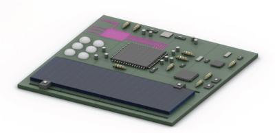
King Abdullah University of Science and Technology (KAUST) researchers have shown how fluid injection of perovskite semiconductors creates microwires to build different optoelectronic devices on a single silicon chip. They have developed a microfluidic pumping technology that can help perovskites be more readily incorporated into silicon-based semiconducting platforms.
 The "lab on a chip" designed at KAUST consists of several perovskite-based optoelectronic devices on one silicon chip, embodying a photodetector, transistor, light-emitting diode and a solar cell, for example. Credit: KAUST and Techxplore
Compared to traditional semiconductors, perovskites are soft and unstable. "This makes it difficult to pattern them using standard lithography methods," says materials scientist Iman Roqan at KAUST. The challenge tackled by Roqan and her colleagues was to adapt microfluidic technologies to manipulate solutions carrying perovskites to create semiconducting microscale wires.
"We are the first researchers to achieve this," says Roqan, adding that the innovation, which has now been patented, will allow several different perovskite-based optoelectronic devices to be located on one silicon chip. For example, a single chip could embody a photodetector, transistor, light-emitting diode and a solar cell to act as the power supply.
To demonstrate the potential of the technique, the team has built a high-performance photodetector.
"Unlike other options, our fabrication method is extremely simple and cost-effective, while avoiding creating waste materials," Roqan says. Some metals used in perovskites are toxic, so avoiding their release into the environment is a significant advantage.
There are still challenges to overcome to advance from this initial proof-of-concept stage. For example, the team is working to bring the stability of the devices up to a standard suitable for large-scale industrial applications. Roqan expects that work currently in progress to achieve this is likely to lead to further patents, while also building more complex demonstration devices.
One of the most likely areas for commercial development is in the growing field of "lab on a chip" technology. This can combine processes such as sensing, signaling, microfluid manipulation and chemical separations and combinations to miniaturize many laboratory procedures used in medicine and biology. With miniaturization comes portability, potentially taking a full testing laboratory process out of the lab and into the outside world.