Perovskites are materials that share a crystal structure similar to the mineral called perovskite, which consists of calcium titanium oxide (CaTiO3).
Depending on which atoms/molecules are used in the structure, perovskites can possess an impressive array of interesting properties including superconductivity, ferroelectricity, charge ordering, spin dependent transport and much more. Perovskites therefore hold exciting opportunities for physicists, chemists and material scientists.
Sensors are devices that detect events that occur in the physical environment (like light, heat, motion, moisture, pressure, and more), and respond with an output, usually an electrical, mechanical or optical signal. The household mercury thermometer is a simple example of a sensor - it detects temperature and reacts with a measurable expansion of liquid. Sensors are everywhere - they can be found in everyday applications like touch-sensitive elevator buttons and lamp dimmer surfaces that respond to touch, but there are also many kinds of sensors that go unnoticed by most - like sensors that are used in medicine, robotics, aerospace and more.
Traditional kinds of sensors include temperature, pressure (thermistors, thermocouples, and more), moisture, flow (electromagnetic, positional displacement and more), movement and proximity (capacitive, photoelectric, ultrasonic and more), though innumerable other versions exist. sensors are divided into two groups: active and passive sensors. Active sensors (such as photoconductive cells or light detection sensors) require a power supply while passive ones (radiometers, film photography) do not.
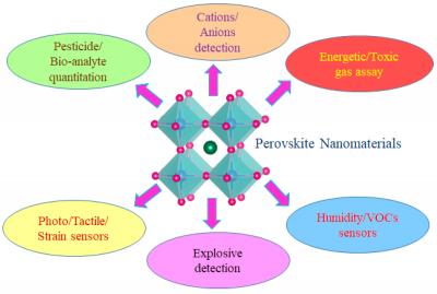
Perovskite materials’ host of exciting properties, such as being rather tolerant to defects (unlike metal chalcogenides) and not requiring surface passivation to retain high quantum yields, make them especially suited for sensing applications. The sensitivity, selectivity, and stability of many perovskite nanomaterials has directed many researchers to devote the most attention to chemical sensors, but perovskites are suitable for other types as well. Perovskites are being studied by numerous research groups for use in various types of sensors.
Researchers examine a perovskite-graphene device for X-ray detection
Researchers at Graphenea, University of Utah and Kairos Sensors have examined a perovskite-based graphene field effect transistor (P-GFET) device for X-ray detection.
The device architecture consisted of a commercially available GFET-S20 chip, produced by Graphenea, with a layer of methylammonium lead iodide (MAPbI3) perovskite spin coated onto the top of it. This device was exposed to the field of a molybdenum target X-ray tube with beam settings between 20 and 60 kVp (X-ray tube voltage) and 30–300 μA (X-ray tube current). Dose measurements were taken with an ion-chamber and thermo-luminescent dosimeters and used to determine the sensitivity of the device as a function of the X-ray tube voltage and current, as well as source-drain voltage.


Researchers report perovskite nanowires-based graphene plasmonic waveguides with low loss and low gain threshold
Researchers at China's Huanghe Science and Technology University, Zhengzhou Normal University and Zhongke Weike Technology (Henan) Co., Ltd have designed a perovskite nanowire-based graphene plasmonic waveguide, where the perovskite nanowire is located on the graphene-insulator-metal (GIM) platform. The findings of this work could have potential applications in plasmonic waveguide-based devices, such as lasers, modulators, sensors, etc.
The finite element method was used in order to investigate the impact of the perovskite nanowire radius, graphene layer thickness, Fermi energy level of the graphene, thickness of the low index dielectric layer, and permittivity of dielectric layer on the mode properties. The results indicate that the hybrid mode exhibits very low propagating loss and ultra-high figure of merit.
Researchers develop ballpoint pens that can write perovskite LEDs on diverse substrates
Researchers from Washington University in St. Louis and Florida State University have developed a versatile, scalable and eco-friendly handwriting approach to draw multicolor perovskite light-emitting diodes and perovskite photodetectors on various substrates, including paper, textiles, plastics, elastomers, rubber and three-dimensional objects.
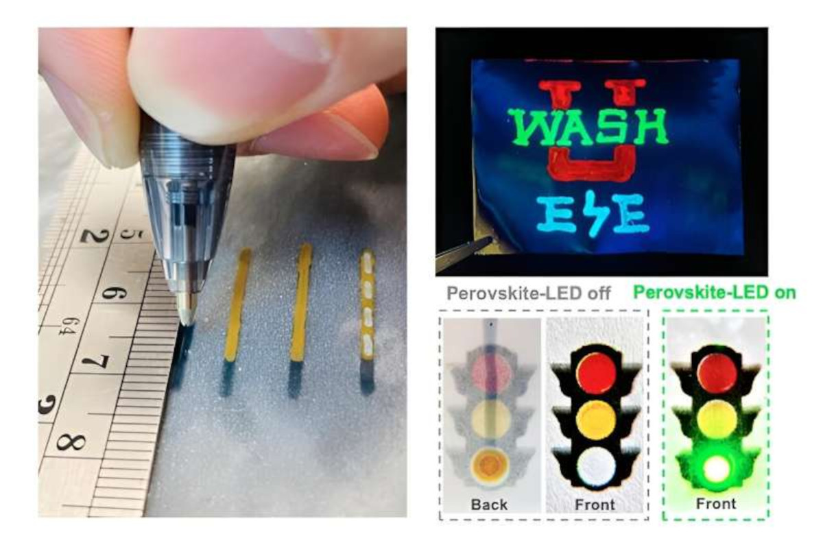
The team's method uses common ballpoint pens filled with newly formulated inks of conductive polymers, metal nanowires and multiple perovskites for a wide range of emission colors. Just like writing with multicolored pens, writing layer-by-layer with these functional inks enables perovskite optoelectronic devices to be realized within minutes.
Researchers develop a platform for integrated spectrometers based on solution-processable semiconductors
Researchers from China's Harbin Institute of Technology and University of Electronic Science and Technology of China have proposed a facile and universal platform to fabricate integrated spectrometers with solution-processable semiconductors by involving the conjugated mode of the bound states in the continuum (conjugated-BIC) photonics.

Acquiring real-time spectral information in point-of-care diagnosis, internet-of-thing, and other lab-on-chip applications requires spectrometers with hetero-integration capability and miniaturized form. Compared to conventional semiconductors integrated by heteroepitaxy, solution-processable semiconductors provide a much-flexible integration platform due to their solution-processability, and, therefore, more suitable for multi-material integrated systems. However, solution-processable semiconductors are usually incompatible with micro-fabrication processes, making them impractical for use in various applications.
Researchers explore how carbon nanotube diameter can influence the performance of photodetector heterojunctions
Researchers from China's Hebei University of Technology and Chinese Academy of Sciences have found that increasing the diameter of single-wall carbon nanotubes (SWCNTs) in SWCNT/perovskite QD heterojunctions can improve the optoelectronic performance of the heterojunction between the two materials.
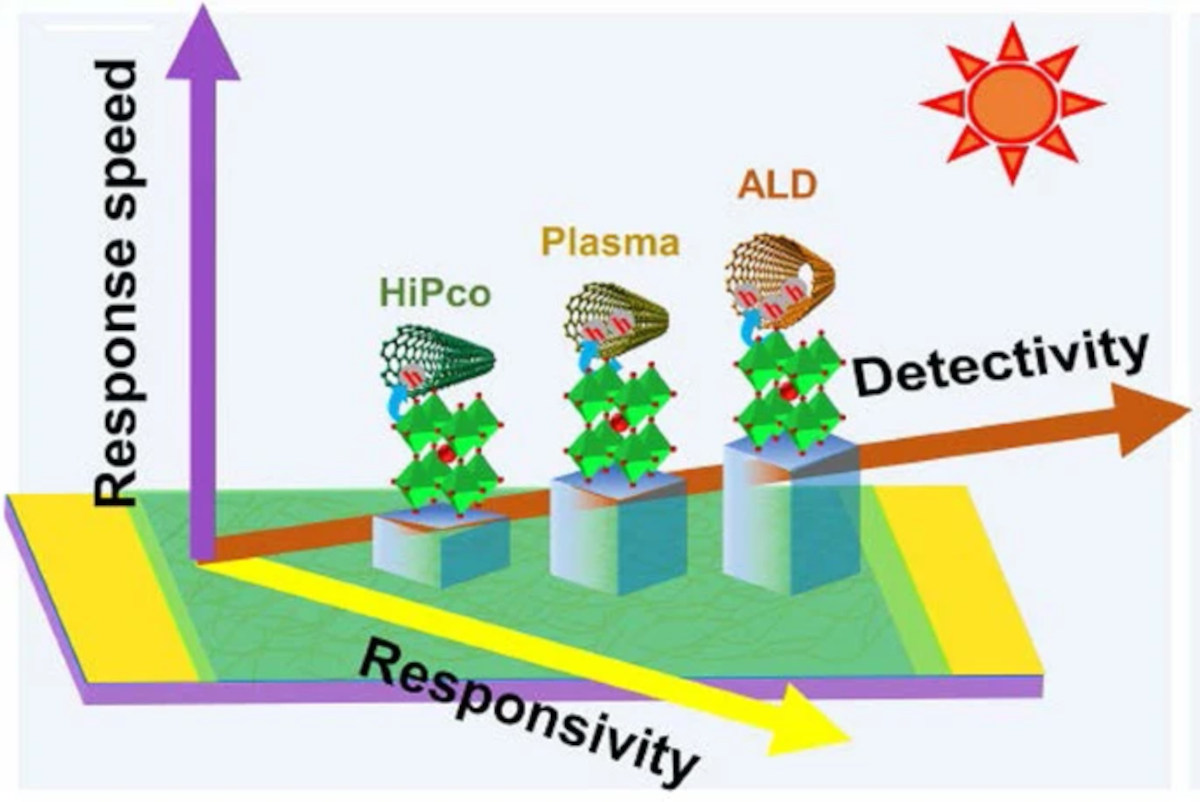
The team systematically tested the performance effects of varying diameters of SWCNTs, a single layer of carbon atoms that form a hexagonal lattice rolled into a seamless cylinder, with different band gaps, or the amount of energy required for an electron to conduct electric current, in heterojunction films with perovskite QDs. Their study indicated that increasing the diameter of SWCNTs improved the responsivity, detectivity and response time of this type of heterojunction film. This effect may be mediated by the enhanced separation and transport of photogenerated excitons, an energy-carrying, neutrally charged electron that combines with a positive electron hole, in the film.
Researchers develop high-performance UV light detector using layered perovskites and textured silicon heterojunction
Researchers from the Zhengzhou University of Light Industry have developed a UV detector of (BA)2PbCl4/textured silicon (BA = n-butylammonium) heterojunction by depositing (BA)2PbCl4 thin film on textured silicon.
High performances of a rapid UV light response (trise = tfall = 0.24 s), high responsivity (8.16 mA/W), and a low detection limit (7.5 μW/cm2) were reportedly obtained from the designed detector, which were ascribed the unique morphology and structure of the detector.
Researchers use perovskites to design LEDs that reveal rot in food before it is visible
Researchers at the Indian Institute of Science Education and Research (IISER) have developed new LEDs which emit light simultaneously in two different wavelength ranges, for a simpler and more comprehensive way to monitor the freshness of fruit and vegetables.
The team explains that modifying the LEDs with perovskite materials causes them to emit in both the near-infrared range and the visible range, a significant development in the contact-free monitoring of food. Angshuman Nag and his team at the Indian Institute of Science Education and Research (IISER) are proposing a perovskite application in LED technology that could simplify the quality control of fresh fruit and vegetables.
EneCoat announces a verification operation of perovskite solar cells in IoT CO2 sensors terminal in Tokyo Metropolitan Government facilities
EneCoat Technologies has announced a collaboration with Macnica, a total service and solution provider in semiconductors, networking, cyber security, and AI/IoT. In addition, the Tokyo Metropolitan Government has announced that it has started verification operation of IoT CO2 sensor terminals equipped with perovskite solar cells (PSCs).
EneCoat has been developing PSCs optimized for IoT terminals in terms of power generation capacity and shape, and has been conducting verification operation of air quality sensors employing PSCs made in collaboration with Macnica since last year. To further advance the efforts, the agreement for the verification operation was signed by Macnica, the Tokyo Metropolitan Government, and EneCoat. By having the Tokyo Metropolitan Government provide offices within the Tokyo Metropolitan Government Building as an environment for air quality monitoring operation, Macnica, the Tokyo Metropolitan Government, and EneCoat will be able to further advance the study and verification of the mass production of IoT sensors equipped with PSCs.
Researchers develop perovskite-based light-field sensor for 3D scene construction
Researchers from the National University of Singapore (NUS), led by Professor Liu Xiaogang from the Department of Chemistry, have developed a perovskite-based 3D imaging sensor that has an extremely high angular resolution, which is the capacity of an optical instrument to distinguish points of an object separated by a small angular distance, of 0.0018o. This innovative sensor operates on a unique angle-to-colour conversion principle, allowing it to detect 3D light fields across the X-ray to visible light spectrum.
Design of the 3D light-field sensor on the basis of pixelated color conversion. Image from study
A light field encompasses the combined intensity and direction of light rays, which the human eyes can process to precisely detect the spatial relationship between objects. Traditional light sensing technologies, however, are less effective. Most cameras, for instance, can only produce two-dimensional images, which is adequate for regular photography but insufficient for more advanced applications, including virtual reality, self-driving cars, and biological imaging. These applications require precise 3D scene construction of a particular space.
Researchers create retina-inspired narrowband perovskite sensor array for panchromatic imaging
Researchers from Pennsylvania State University have developed a narrowband (NB) imaging sensor combining R/G/B perovskite NB sensor array (mimicking the R/G/B photoreceptors in the eye) with a neuromorphic algorithm (mimicking the intermediate neural network of the human visual system) for high-fidelity panchromatic imaging.
A photo of a perovskite NB PD array made in this work. Image from study
Compared to commercial sensors, the team used perovskite “intrinsic” NB photodetectors to exempt the complex optical filter array. In addition, They used an asymmetric device configuration to collect photocurrent without external bias, enabling a power-free photodetection feature. These results presented a promising design for efficient and intelligent panchromatic imaging.

