Perovskites are materials that share a crystal structure similar to the mineral called perovskite, which consists of calcium titanium oxide (CaTiO3).
Depending on which atoms/molecules are used in the structure, perovskites can possess an impressive array of interesting properties including superconductivity, ferroelectricity, charge ordering, spin dependent transport and much more. Perovskites therefore hold exciting opportunities for physicists, chemists and material scientists.
Sensors are devices that detect events that occur in the physical environment (like light, heat, motion, moisture, pressure, and more), and respond with an output, usually an electrical, mechanical or optical signal. The household mercury thermometer is a simple example of a sensor - it detects temperature and reacts with a measurable expansion of liquid. Sensors are everywhere - they can be found in everyday applications like touch-sensitive elevator buttons and lamp dimmer surfaces that respond to touch, but there are also many kinds of sensors that go unnoticed by most - like sensors that are used in medicine, robotics, aerospace and more.
Traditional kinds of sensors include temperature, pressure (thermistors, thermocouples, and more), moisture, flow (electromagnetic, positional displacement and more), movement and proximity (capacitive, photoelectric, ultrasonic and more), though innumerable other versions exist. sensors are divided into two groups: active and passive sensors. Active sensors (such as photoconductive cells or light detection sensors) require a power supply while passive ones (radiometers, film photography) do not.
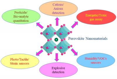
Perovskite materials’ host of exciting properties, such as being rather tolerant to defects (unlike metal chalcogenides) and not requiring surface passivation to retain high quantum yields, make them especially suited for sensing applications. The sensitivity, selectivity, and stability of many perovskite nanomaterials has directed many researchers to devote the most attention to chemical sensors, but perovskites are suitable for other types as well. Perovskites are being studied by numerous research groups for use in various types of sensors.
Perovskite-based sensors can help detect harmful pesticides and toxins
Various dangerous chemicals are currently used for agriculture and industry, including fumigants like methyl iodide, which is used to control insects and fungi. The wrong amounts or incorrect use of these fumigants can be harmful to people and degrade the ozone layer. As it’s invisible and doesn’t smell, it’s hard to tell whether there are dangerous amounts of methyl iodide present, and until now the best way to test for it was in a laboratory using expensive, complicated equipment, which isn’t practical in many real-world settings. Some cheaper, lightweight detection methods have been tried, but they didn’t have enough sensitivity and took too long to deliver results.
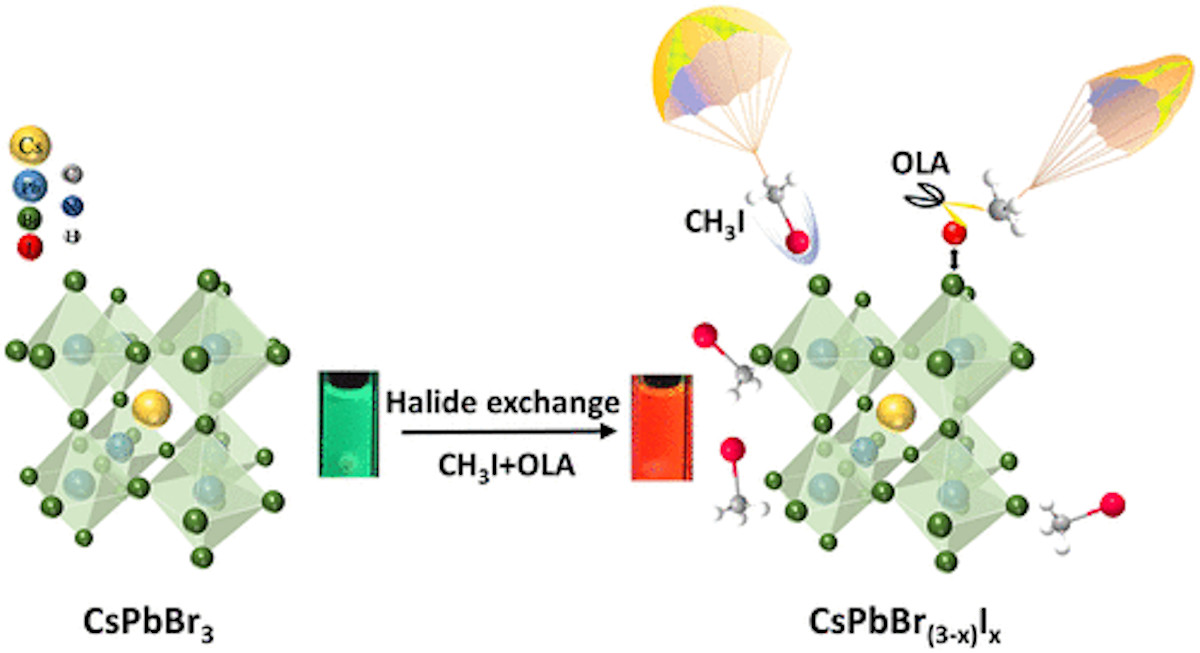
Now, a research team led by the ARC Centre of Excellence in Exciton Science, along with Australia’s national science agency CSIRO and the Department of Defense, has found a perovskite-based way to detect methyl iodide, with the accuracy, flexibility and speed necessary for practical use. This new sensing mechanism is also versatile enough for use in detecting a wide range of fumigants and chemical warfare agents.


Researchers design novel X-ray photodetectors based on perovskites on top of graphene
A team of scientists, led by László Forró from the School of Basic Sciences at the Ecole Polytechnique Federale de Lausanne (EPFL) in Switzerland, has developed a new X-Ray Photodetector based on perovskites and graphene.
Using 3D aerosol jet-printing technology, the team designed a new technique for creating highly efficient x-ray photodetectors that can be easily added to standard microelectronic circuits, creating more powerful medical imaging devices that can deliver better scan qualities.
Researchers show lead-free quadruple perovskite nanocrystals' potential for photovoltaic and optoelectronic applications
A research group, led by Prof. HAN Keli from the Dalian Institute of Chemical Physics of the Chinese Academy of Sciences, recently revealed the luminescence enhancement mechanism of a series of new lead-free quadruple halide perovskite nanocrystals, and prepared high-performance photodetectors.
The researchers reported a series of quadruple perovskite colloidal nanocrystals with ordered vacancies. By alloying Cs4MnBi2Cl12 nanocrystals, the fluorescence quantum yield could be increased by nearly 100 times.
EPFL team develops perovskite material that can detect gamma rays
Researchers at Ecole Polytechnique Fédérale de Lausanne (EPFL), assisted by teams at Croatia's University of Split, have developed a perovskite that can detect gamma rays.
 method of large MAPbBr3 crystals image") The 'oriented crystal'crystal growth' (OC2G) method of large MAPbBr3 crystals . a) Growing of large crystals by the suspended seed crystal; b,c) The consecutive steps of fusing together individual single crystals into a large crystal. Image by EPFL
The 'oriented crystal'crystal growth' (OC2G) method of large MAPbBr3 crystals . a) Growing of large crystals by the suspended seed crystal; b,c) The consecutive steps of fusing together individual single crystals into a large crystal. Image by EPFL
"This photovoltaic perovskite crystal, grown in this kilogram size, is a game changer," says EPFL's Professors Lászlo Forró. "You can slice it into wafers, like silicon, for optoelectronic applications, and, in this paper, we demonstrate its utility in gamma-ray detection."
Perovskite-based optical sensor mimics the human eye
Researchers at Oregon State University have reported recent advances with a new type of perovskite-based optical sensor that more closely mimics the human eye's ability to perceive changes in its visual field. The sensor could be highly beneficial for fields like image recognition, robotics and artificial intelligence.
The team explained that previous attempts to build a human-eye type of device, called a retinomorphic sensor, have relied on software or complex hardware. However, the new sensor's operation is part of its fundamental design, using ultrathin layers of perovskite semiconductors that change from strong electrical insulators to strong conductors when placed in light.
New perovskite detector shows promise for medical diagnostics and homeland security
Northwestern University researchers have developed new perovskite-based devices to assist in the detection and identification of radioactive isotopes. This method could allow the identification of legal versus illegal gamma rays - such detectors are critical for national security, where they're used to detect illegal nuclear materials smuggled across borders and aid in nuclear forensics, as well as in medical diagnostics imaging.
Using cesium lead bromide in the form of perovskite crystals, the research team found they were able to create highly efficient detectors in both small, portable devices for field researchers and very large detectors.
Perovskite-based photodiode could open the door to next-gen sensors that detect circularly polarized light without filters
Under the Japan Science and Technology Agency (JST) Strategic Basic Research Programs, researcher Ayumi Ishii (Toin University of Yokohama, specially appointed lecturer) has developed a photodiode using a crystalline film composed of lead perovskite compounds with organic chiral molecules to detect circularly polarized light without a filter.
A technology to detect "polarization," or oscillation direction of light, can visualize object surfaces with damages, foreign objects, and distortions. Furthermore, detection of "circularly polarized light," or rotating electric field of light makes it possible for us to identify stress intensity and distribution of objects. Conventional photodiodes for camera or sensor applications cannot detect polarization of light directly, and therefore, various types of filters must be attached on top of the device to separate the information of polarization spatially. These structures cause substantial losses of sensitivity and resolution in the light detection, especially detection of circularly polarized light is heretofore considered difficult. Thus, it has been much sought-after to develop a new sensor for detection of circularly polarized light without any filters.
Korean team designs a new kind of liquid scintillator via hybridizing perovskite nanocrystals with organic molecules
A team of scientists, led by Professors Hyunsik Im, Hyungsang Kim and Jungwon Kwak from Dongguk University and Asan Medical Center in Korea,have developed perovskite metal halide nanocrystals based hybrid materials with high quantum yields for efficient X-ray detection and high-resolution X-ray imaging.
Using the hybrid nanomaterial scintillators, they designed a scalable and cost-effective X-ray detector panel in liquid form. The hybrid nanomaterial scintillator works under X-ray irradiation typically employed in both diagnosis and treatment. More interestingly, the hybrid scintillator has a faster scintillation decay process over the conventional scintillators, which is beneficial for digital motion X-ray. The reported method and scintillation mechanism will be extended to enhance the quantum yield of various types of scintillators, enabling low-dose radiation detection in various fields including fundamental science and imaging.
New production method yields flexible single-crystal perovskite films with controlled area, thickness, and composition
Scientists at UC San Diego have developed a new method to fabricate perovskites as single-crystal thin films, which are more efficient for use in solar cells and optical devices than the current state-of-the-art polycrystalline forms of the material.
Their fabrication method - which uses standard semiconductor fabrication processes - results in flexible single-crystal perovskite films with controlled area, thickness, and composition. These single-crystal films showed fewer defects, greater efficiency, and enhanced stability than their polycrystalline counterparts, which could lead to the use of perovskites in solar cells, LEDs, and photodetectors.
Graphene boosts perovskite single crystal photodetector performance
The performance of photodetectors based on perovskite polycrystalline thin films is still considered to be at a distance from expected values. One reason is that the carrier transport at the interface is easily affected by grain boundaries and grain defects. Many research groups have tried to combine perovskite polycrystalline thin films with high-mobility, two-dimensional materials to improve device performance, and have achieved promising results, but the negative effects of perovskite polycrystalline grain boundaries still remain.
To solve this problem, a team led by Assoc. Prof. Yu Weili from Changchun Institute of Optics, Fine Mechanics and Physics (CIOMP) of the Chinese Academy of Sciences, and Prof. GUO Chunlei from the University of Rochester synthesized a low-surface-defect-density CH3NH3PbBr3 microplate through the inverse temperature crystallization strategy. They prepared an effective vertical structure photodetector combining a high-quality perovskite single crystal with monolayer graphene with high carrier mobility.

