Researchers create a field-effect transistor using a single-crystal, “paint-on” perovskite

An international team of researchers, led by Aram Amassian at North Carolina State University, has demonstrated the construction of field-effect transistors using a single crystal, hybrid perovskite semiconductor.
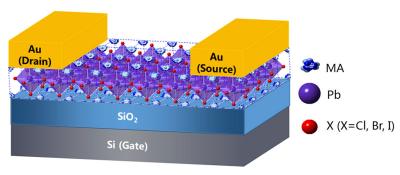
Researchers create a field-effect transistor using a single-crystal, 'paint-on' perovskite image

While the design of perovskite solar cells has matured to the point of near-commercialization, making hybrid perovskites function as field-effect transistors has been more of a challenge. This is in part due to the fact that perovskite films typically consist of multiple crystals with random orientations that include grain boundaries and various kinds of defects in their atomic crystal lattices. These often limit how well charge carriers (electrons or 'holes') can move through them.
Read the full story Posted: Jan 17,2019

Researchers integrate single-crystal hybrid perovskites into electronics

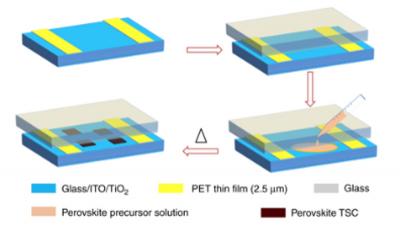
An international team of researchers, including ones from KAUST, the Guo China-US Photonics Laboratory, the University of Rochester and the University of New South Wales, has developed a technique that allows single-crystal hybrid perovskite materials to be integrated into electronics. The team stated that this achievement opens the door to new research into flexible electronics and potentially reduced manufacturing costs for electronic devices.

Researchers succeed in integrating single-crystal hybrid perovskites into electronics image

Challenges in integrating single-crystal hybrid perovskites into electronic devices, such as transistors, have spurred much research focus. The main challenge in incorporating single-crystal hybrid perovskites into electronics stems from the fact that these macroscopic crystals, when synthesized using conventional techniques, have rough, irregular edges. This makes it difficult to integrate with other materials in such a way that the materials make the high-quality contacts necessary in electronic devices.

Read the full story Posted: Dec 19,2018

Researchers demonstrate controlled epitaxial growth of all inorganic lead-free halide perovskites

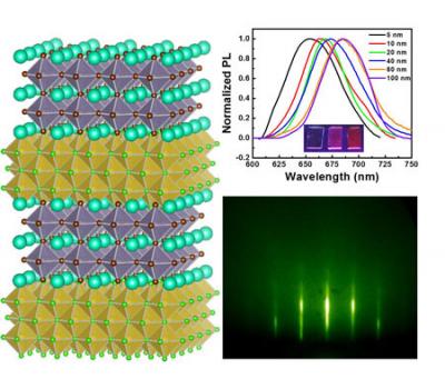
A research team composed of scientists from Michigan State University and University of Michigan has deployed a new approach to growing all inorganic lead-free halide perovskites.

Perovskite quantum wells scheme image

"Epitaxial growth has long since revolutionized the study of many electronic materials including silicon, oxide perovskites, and III-V semiconductors," said Richard Lunt, an Associate Professor at Department of Chemical Engineering and Materials Science, Michigan State University who has supervised the project. "There is very little known about the epitaxial growth of halide perovskites, but these exciting materials hold enormous potential. This has motivated us to explore this entirely new research area."

Read the full story Posted: Apr 02,2018

World's first 2D sheets of organic-inorganic hybrid perovskites grown from a solution

Researchers at the Department of Energy's Lawrence Berkeley National Laboratory have succeeded in growing atomically thin 2D sheets of organic-inorganic hybrid perovskites from a solution. The sheets are claimed to be of high quality and large in area.

The scientists state that this is the first example of 2D atomically thin nanostructures made from ionic materials and that the results of this study open up opportunities for fundamental research on the synthesis and characterization of atomically thin 2D hybrid perovskites and introduce a new family of 2D solution-processed semiconductors for nanoscale optoelectronic devices, such as field effect transistors and photodetectors.

Read the full story Posted: Sep 29,2015