October 2023

Researchers report perovskite solar cell with ultrathin protective TMO buffer layers

Researchers from the University of Rome Tor Vergata, ENEA and CNR-ISM have used protective buffer layers in perovskite solar cells to mitigate damage during the sputtering of indium tin oxide in the production process. The scientists claim the buffer layers were able to achieve this without damaging the cell’s average visible transmittance.

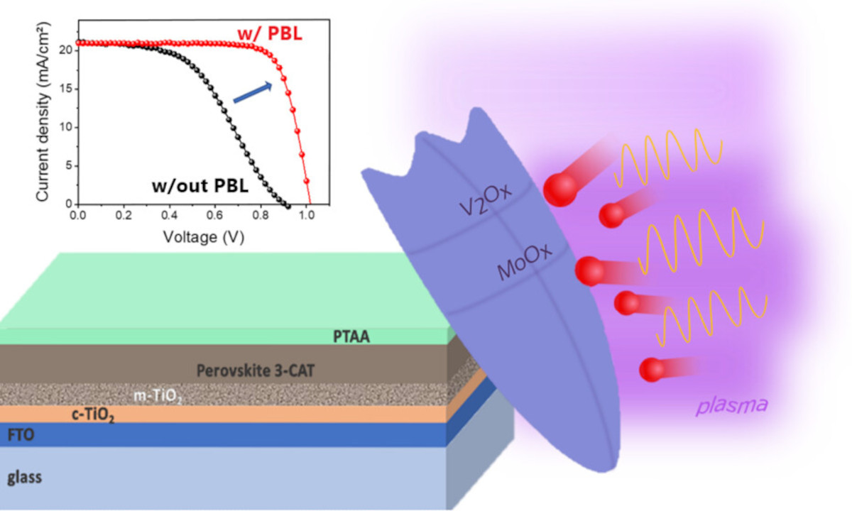
The cell utilizes buffer layers made of transition metal oxides (TMOs) intended to protect the cell during the sputtering of indium tin oxide (ITO) in the cell production process. The scientists tested, in particular, two different evaporated transition metal oxides (TMOs) – molybdenum oxide (MoOx) and vanadium oxide (V2Ox)  and found the former provided the best performance.

Read the full story Posted: Oct 31,2023

Researchers develop improved method for 2D perovskite crystals via progressive transformation of quantum well thickness

A research team, led by Rice University chemical and biomolecular engineer Aditya Mohite and collaborators at Northwestern University, the University of Pennsylvania and the University of Rennes, reported a process that yields 2D perovskite-based semiconductor layers of ideal thickness and purity by controlling the temperature and duration of the crystallization process.

Known as kinetically controlled space confinement, the process could help improve the stability and reduce the cost of halide perovskite-based emerging technologies like optoelectronics and photovoltaics.

Read the full story Posted: Oct 28,2023

A look into the perovskite solar industry by application

The perovskite solar industry is emerging and becoming a vibrant industry, with dozens of companies that are developing and starting to produce perovskite-based and perovskite-enhanced solar panels, for many applications.

While the industry is still at an early stage, we can see that almost half (43%) of the active perovskite developers are focused on solutions for outdoor applications – mainly roof top and utility scale applications – for generating electricity on a large scale, a replacement for current silicon-based solutions. While this is a challenging area (requires low cost, high performance and very high stability), the size of this market is large and proven. Perovskite has some inherent advantages in this area – low weight, low cost, high return on investment, high efficiency and excellent light absorption properties.

Read the full story Posted: Oct 26,2023

Researchers use hole-selective contact on light-managing textured substrates for efficient and stable inverted PSCs

Inverted perovskite solar cells (PSCs) can deliver enhanced operating stability compared to their 'normal'-structure counterparts. To improve efficiency further, it is vital to combine effective light management with low interfacial losses. Now, scientists at Northwestern University, University of Kentucky, North Carolina State University, University of Toronto, Ecole Polytechnique Fédérale de Lausanne (EPFL) and Peking University have developed a conformal self-assembled monolayer (SAM) as the hole-selective contact on light-managing textured substrates. 

The team reported that molecular dynamics simulations indicate cluster formation during phosphonic acid adsorption leads to incomplete SAM coverage. They devised a co-adsorbent strategy that disassembles high-order clusters, thus homogenizing the distribution of phosphonic acid molecules, thereby minimizing interfacial recombination and improving electronic structures.

Read the full story Posted: Oct 24,2023

Researchers report perovskite nanowires-based graphene plasmonic waveguides with low loss and low gain threshold

Researchers at China's Huanghe Science and Technology University, Zhengzhou Normal University and Zhongke Weike Technology (Henan) Co., Ltd have designed a perovskite nanowire-based graphene plasmonic waveguide, where the perovskite nanowire is located on the graphene-insulator-metal (GIM) platform. The findings of this work could have potential applications in plasmonic waveguide-based devices, such as lasers, modulators, sensors, etc.

The finite element method was used in order to investigate the impact of the perovskite nanowire radius, graphene layer thickness, Fermi energy level of the graphene, thickness of the low index dielectric layer, and permittivity of dielectric layer on the mode properties. The results indicate that the hybrid mode exhibits very low propagating loss and ultra-high figure of merit. 

Read the full story Posted: Oct 23,2023

Japan's JGC declares its aim to bring bendable perovskite solar cells to building walls by 2026

Japanese engineering company JGC Holdings has stated its plans to commercialize (by 2026) bendable perovskite solar cells that can be installed on curved surfaces, such as chemical tanks, shop walls or domed buildings.

JGC plans to use perovskite solar cells developed by EneCoat Technologies, a Kyoto University startup in which it has a stake. As a first step, the company will test the solar cells on the roof of a warehouse in Tomakomai, Hokkaido, next year. The aim is to start large-scale power generation by 2026, with projected sales of tens of billions of yen (10 billion yen equals $66.7 million) targeted for 2030.

Read the full story Posted: Oct 22,2023

Researchers address the thermal instability of perovskite solar cells by developing a layer of nickel oxide nanoparticles, topped by a SAM

In an effort to tackle the challenge of perovskite solar cells' thermal instability, researchers at City University of Hong Kong (CityU), National Renewable Energy Laboratory (NREL) and Huazhong University of Science and Technology have developed a unique type of self-assembled monolayer, or SAM for short, and anchored it on a nickel oxide nanoparticles surface as a charge extraction layer. This method dramatically enhanced the thermal robustness of perovskite solar cells, according to Professor Zhu Zonglong of the Department of Chemistry at CityU.

“By introducing a thermally robust charge extraction layer, our improved cells retain over 90% of their efficiency, boasting an impressive efficiency rate of 25.6%, even after operated under high temperatures, around (65℃) for over 1,000 hours. This is a milestone achievement,” said Professor Zhu.

Read the full story Posted: Oct 21,2023

The advantages of perovskite solar technology

Silicon-based solar cells currently dominate the solar market. It is a proven technology, with established manufacturing processes. However, it is also quite expensive to produce, yields rigid cells and has an estimated efficiency limit of around 29%. In recent years, perovskite-based solar technologies have been drawing a lot of attention, and many academics and companies believe they are the future of the solar industry.

Perovskite Solar Cell (PSC) technology is a photovoltaic (PV) technology based on the use of perovskite materials, mostly in the light-absorbing layers of the cell. There are many types of perovskite materials, and several processes used to deposit these materials to create efficient solar panels. PSCs have potential for creating solar panels that are easily deposited onto most surfaces, including flexible and textured ones. They can also be lightweight, cheap to produce, and more efficient than silicon-based solar cells (efficiencies in the lab have already crossed 30%). 

The major advantages of perovskite-based solar cells are factors of performance, applicability and sustainability:

Read the full story Posted: Oct 19,2023

Cosmos Innovation raises $19.7 million for AI-supported development of tandem perovskite-silicon solar cells

Cosmos Innovation, a company that relies on its AI platform called Mobius for "revolutionizing the approach to solar and semiconductor process development", has announced raising $19.7 million in total funding. The funding will support the company's different approach to developing perovskite silicon tandem solar cell technology.

The funding coincides with Cosmos Innovation's unveiling of Mobius, its pioneering AI recipe optimization platform. Mobius has reportedly been demonstrated across various sectors, including solar, silicon carbide, advanced data center chips and advanced packaging. This platform fuels Cosmos Innovation's ambitious endeavor: construction of the world's first self-learning fab in the solar and semiconductor space.

Read the full story Posted: Oct 16,2023

Researchers design large-area perovskite-silicon tandem device with record efficiency of 25.1%

Researchers at the University of North Carolina at Chapel Hill and Arizona State University and have designed a large-area perovskite-silicon tandem solar cell that achieved a steady-state power conversion efficiency of 25.1% for tandem devices with a large aperture area of 24 cm2.

The team set out to overcome shunting, which is a common issue when scaling up perovskite solar technologies from small-area cells to large-area devices. “Shunts” in PV cells create alternate pathways for a solar-generated charge, leading to power losses. Reduced shunt resistance is associated with multiple forms of module degradation and failure, including hotspots and potential-induced degradation.

Read the full story Posted: Oct 16,2023