Researchers from the University of Toledo, NREL and the University of Colorado Boulder have designed highly efficient, bifacial, single-junction perovskite solar cells based on a p-i-n (or inverted) architecture. In this work, the team showed that bifacial perovskite photovoltaics technology has the potential to outperform its monofacial counterparts.
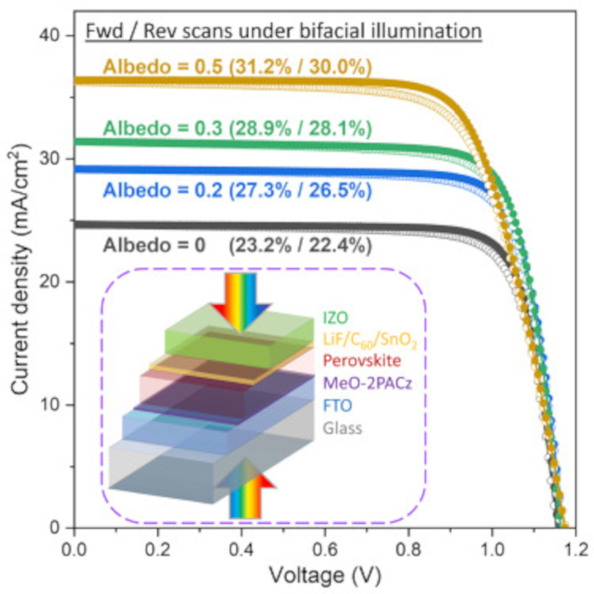
The team used optical and electrical modeling to guide the optimization of the transparent conducting rear electrode and perovskite absorber layer using a p-i-n device architecture, achieving a high bifaciality of about 91%–93% and a high front-side illumination PCE of over 23%. Under concurrent bifacial measurement conditions, the equivalent, stabilized bifacial power output densities were 26.9, 28.5, and 30.1 mW/cm2 under albedos of 0.2, 0.3, and 0.5, respectively.
The dual nature of a bifacial solar cell enables the capture of direct sunlight on the front and the capture of reflected sunlight on the back, allowing this type of device to outperform its monofacial counterparts.
Past bifacial perovskite solar cells yielded devices considered inadequate in comparison to monofacial cells. Ideally, the NREL researchers noted, a bifacial cell should have a front-side efficiency close to the best-performing monofacial cell and a similar back-side efficiency. The researchers were able to make a solar cell where the efficiency under illumination from both sides are close together. The lab-measured efficiency of the front illumination reached above 23%. From the back illumination, the efficiency was about 91%–93% of the front.
Before fabricating the cell, researchers used on optical and electrical simulations to determine the necessary thickness. The perovskite layer on the front of the cell had to be sufficiently thick to absorb most of the photons from a certain part of the solar spectrum, but a perovskite layer that is too thick can block the photons. On the back of the cell, the team had to determine the ideal thickness of the rear electrode to minimize resistive loss.
According to the team, simulations guided the design of the bifacial cell, and without that assistance the researchers would have had to experimentally produce cell after cell to determine the ideal thickness. They found the ideal thickness for a perovskite layer is around 850 nanometers.


To evaluate the efficiency gained through bifacial illumination, the researchers placed the cell between two solar simulators. Direct light was aimed at the front side, while the back side received reflected light. The efficiency of the cell climbed as the ratio of reflected light to the front illumination increased.
While researchers estimate that a bifacial perovskite solar module would cost more to manufacture than a monofacial module, over time bifacial modules could end up being better financial investments because they generate 10%–20% more power.

