Researchers from the Ulsan National Institute of Science and Technology (UNIST) have teamed up with researchers from Daegu Gyeongbuk Institute of Science and Technology (DGIST) to develop a patterning technique for the production of perovskite nanocrystal displays which are ultra-thin and high-resolution. The production involves a very simple stamp-like printing process that will facilitate the commercialization of the new technique.
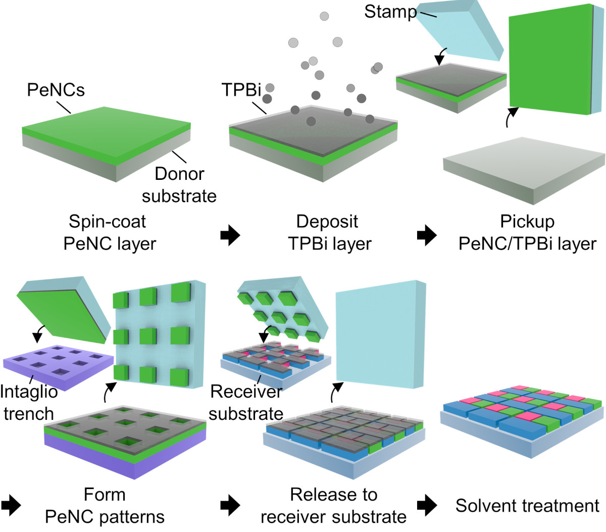
Double-layer transfer printing process with RGB pixelated arrays of PeNCs. Image from Science Advances
The technique reportedly enabled the team to produce a display with RGB pixel patterns of 2,550 pixels per inch, which is about 400 percent higher resolution than the latest high-end smartphones.
Perovskite nanocrystals are a class of nanocrystals regarded as a next-generation material for ultra-high-resolution quantum dot displays. They can be used as a material capable of producing thin and curved high-resolution displays, but nanocrystal displays tend to be chemically and physically unstable, requiring complicated equipment and processes to manufacture perovskite displays.
Conventional circuit boards and semiconductors for perovskite light emitting diodes (LEDs) usually entail a series of etching processes to cut away unwanted circuit parts and leave very finely designed circuit boards. Such methods require complicated procedures with a high defect rate. The newly developed technique allows manufacturers to simply "stamp" layers of perovskite nanocrystal LEDs (PeLEDs) for easy and quick production. The printed PeLEDs have outstanding electroluminescence characteristics and can be adhered to curved surfaces like the skin or a leaf. It can also withstand forces created by twisting and bending.
"By greatly increasing the resolution of the PeLED-based displays, we expect them to be used in a wide range of sectors. The display will help increase the immersive experience of virtual reality and augmented reality devices by actualizing screens with higher resolutions than conventional screens," UNIST researcher Choi Moon-kee said in a statement.

