Researchers at the Karlsruhe Institute of Technology (KIT), Institute for Solar Energy Research Hamelin (ISFH) and Leibniz University Hannover have designed triple-junction perovskite–perovskite–silicon solar cells with a record power conversion efficiency of 24.4%.
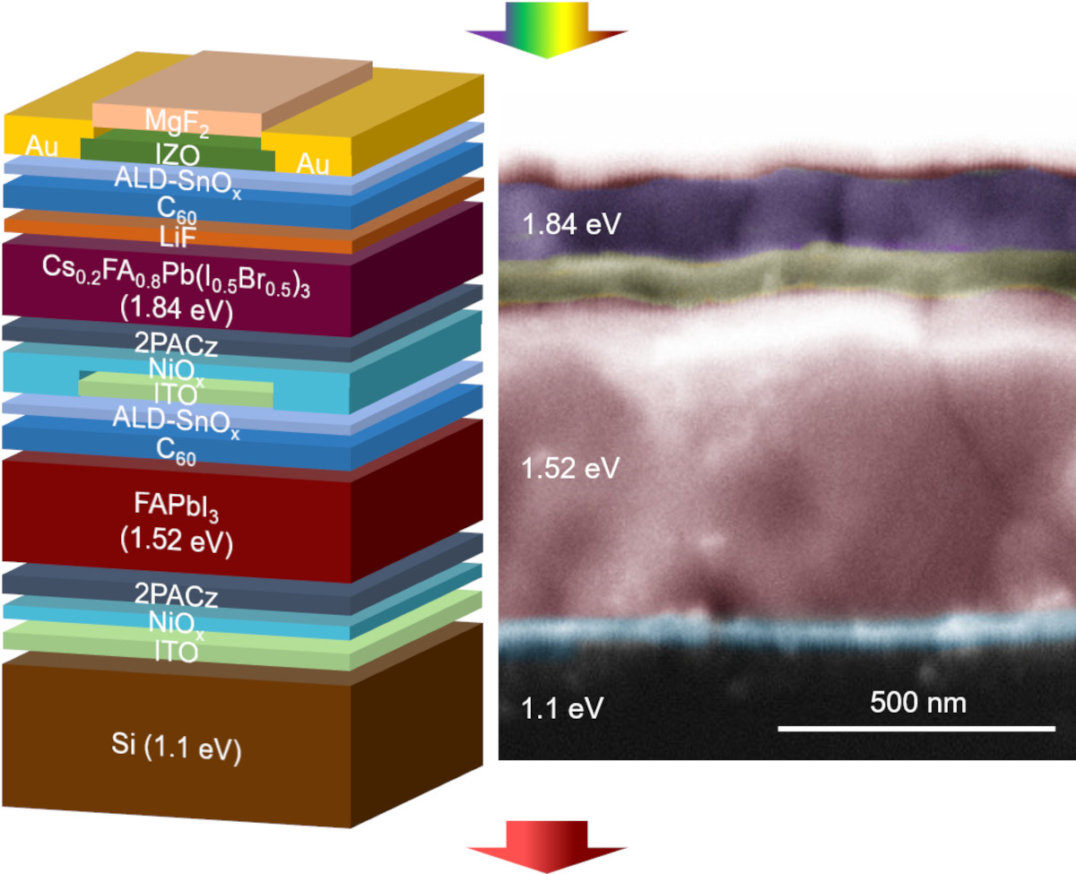
Schematic of the solar cell. Image from Energy & Environmental Science
Optimizing the light management of each perovskite sub-cell (∼1.84 and ∼1.52 eV for top and middle cells, respectively), the team maximized the current generation up to 11.6 mA cm−2. Key to this achievement was the development of a high-performance middle perovskite sub-cell, employing a stable pure-α-phase high-quality formamidinium lead iodide perovskite thin film (free of wrinkles, cracks, and pinholes). This enabled a high open-circuit voltage of 2.84 V in a triple junction. Non-encapsulated triple-junction devices retain up to 96.6% of their initial efficiency if stored in the dark at 85 °C for 1081 h.
Multi-junction perovskite-based photovoltaics using three or more junctions have thus far been lagging behind in performance compared to monolithic perovskite-based double-junction solar cells. According to the team, the key challenges in processing triple-junction architectures are the sequential processing of high-quality perovskite thin films in the increasingly complex multi-layer architecture, light management and current matching of the monolithically interconnected sub-cells, as well as the development of low-loss tunnel/recombination junctions. The scientists stressed that to date, the most critical junction is the middle perovskite subcell, since it is processed on top of the Si bottom cell and needs to withstand the subsequent processing of the wide-bandgap (WBG) perovskite top cell.
In their recent study, the researchers explained that the cell was based on a perovskite top cell with an energy bandgap of 1.84 eV, a perovskite middle cell with bandgap of 1.52 eV, and a silicon bottom cell with a bandgap of 1.1 eV. The bottom cell had a thickness of 200 μm-thick. It was etched with potassium hydroxide, and was based on electron-collecting poly-Si on oxide (POLO) junctions. For the middle and top devices, the scientists used one of the most promising halide perovskites – the α-formamidinium lead iodide known as α-FAPbI3. The recombination junctions were formed by sputtered indium tin oxide (ITO) layers. ITO also serves as anchoring oxide for the sequential hole transport layer (HTL), especially for the double HTLs of NiOx/self-assembled monolayer (SAM). Also, a double HTL based on a combination of sputtered nickel(II) oxide (NiOx) and carbazole (2PACz) was used in both perovskite subcells, reportedly offering an excellent charge carrier extraction, a robust barrier for the solvents of perovskite precursor, and a very good yield for the devices.
Tested under standard illumination conditions, the triple-junction cell achieved a power conversion efficiency of 24.4%, an open-circuit voltage of 2.84 V, a short-circuit current of 11.6 mA cm–2, and a fill factor of 74%. The research group stated this is the highest efficiency ever reported to date for this kind of triple-junction device. The cell was also able to retain 96.6% of the initial efficiency in dark storage aging at 85 C for 1,081 h. Using optical simulations and experimental optimizations in triple junction, the team was able to minimize current mismatch and maximize current generation.


