Researchers from EMPA (Swiss Federal Laboratories for Materials Science and Technology), University of Cantabria and National Tsing Hua University have created a bifacial perovskite-CIGS tandem solar cell and developed a new low-temperature production process resulting in record efficiencies of 19.8% for front and 10.9% for rear illumination.
The idea is collecting direct sunlight, as well as its reflection via the rear end of the solar cell, which should increase the yield of energy the cell produces. Potential applications are, for instance, building-integrated photovoltaics, agrivoltaics – the simultaneous use of areas of land for both photovoltaic power generation and agriculture – and vertically or high-tilt installed solar modules on high-altitude grounds.
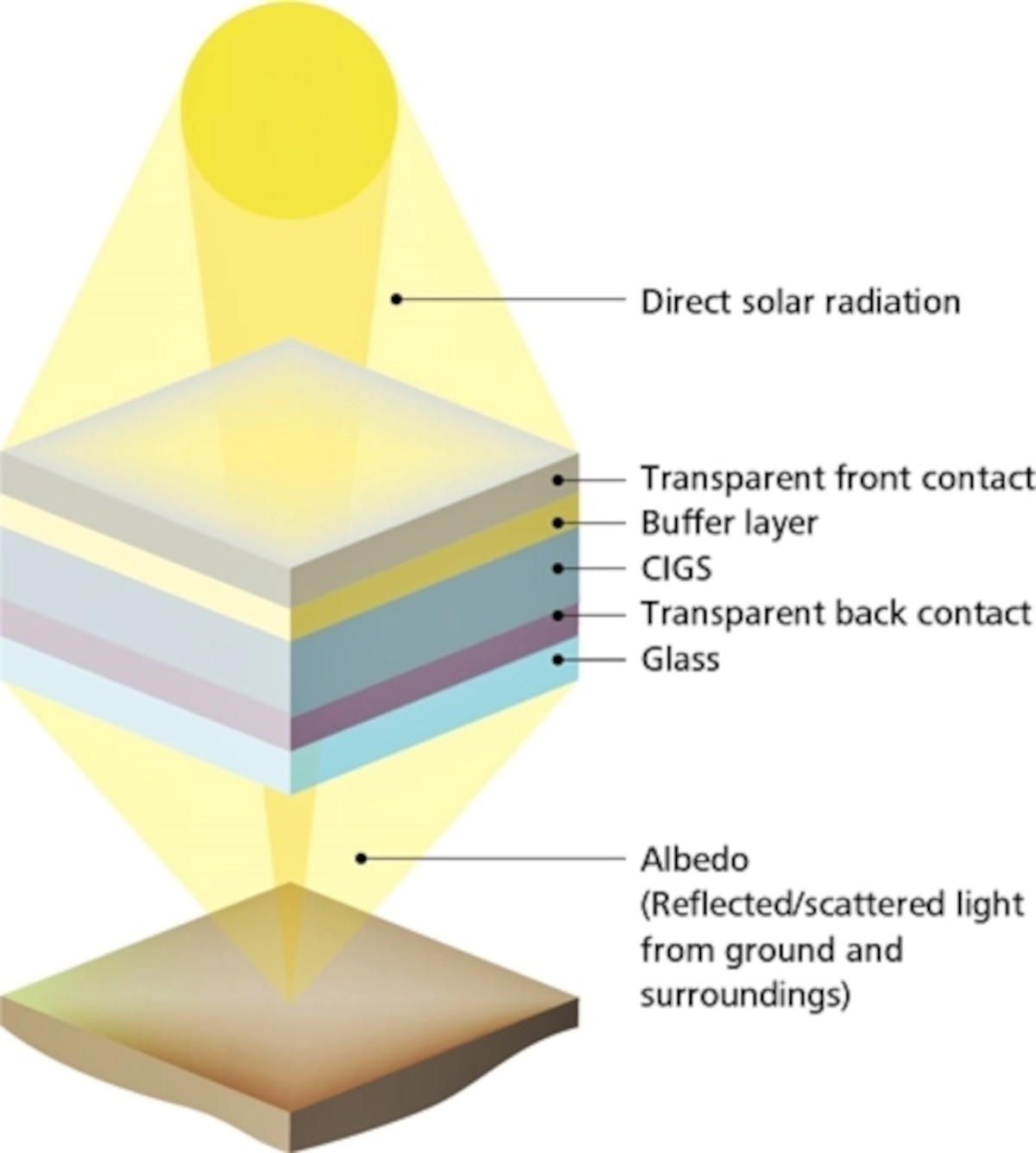
According to the International Technology Roadmap of Photovoltaics, bifacial solar cells could capture a market share of 70% of the overall photovoltaics market by 2030. Although bifacial solar cells based on silicon wafers are already on the market, thin film solar cells have so far lagged behind. This is, at least in part, due to the rather low efficiency of bifacial CIGS thin film solar cells caused by a critical bottleneck problem: For any bifacial solar cell to be able to collect reflected sunlight at the rear side, an optically transparent electrical contact is a prerequisite. This is achieved by using a transparent conductive oxide (TCO) that replaces the opaque back contact in conventional – i.e. mono-facial – solar cells made of molybdenum.
This has proven to be very problematic. High-efficiency CIGS solar cells are generally produced by a high-temperature deposition process, i.e. above 550 degrees. At these temperatures, however, a chemical reaction occurs between the gallium (of the CIGS layer) and the oxygen of the transparent back contact – an oxide. The resulting gallium oxide interface layer blocks the flow of sunlight-generated current and thus reduces the energy conversion efficiency of the cell. The highest values achieved so far in a single cell are 9.0% for the front side and 7.1% for the rear side.
"It’s really difficult to have a good energy conversion efficiency for solar cells with both front and rear transparent conducting contacts," says Ayodhya N. Tiwari, who leads Empa's Thin Film and Photovoltaics lab.
So, PhD student Shih-Chi Yang in the group of Romain Carron in Tiwari's lab developed a new low-temperature deposition process that should produce much less of the detrimental gallium oxide – ideally none at all. They used a tiny amount of silver to lower the melting point of the CIGS alloy and to obtain absorber layers with good electronic properties at just 353 degrees deposition temperature. And sure enough, when they analyzed the multilayer structure with high-resolution transmission electron microscopy, with the help of Tiwari's former postdoc Tzu-Ying Lin, currently at National Tsing Hua University in Taiwan, the team could not detect any gallium oxide at the interface at all.


This was also reflected by a drastically improved energy conversion efficiency: The cell yielded values of 19.8% for front illumination and 10.9% for rear illumination that had been independently certified by the Fraunhofer Institute for Solar Energy Systems (ISE) in Freiburg/Germany – in the very same cell on a glass substrate.
In addition, the team also succeeded in fabricating, for the first time, a bifacial CIGS solar cell on a flexible polymer substrate, which – due to their light weight and flexibility – widens the spectrum of potential applications.
And finally, the researchers combined two photovoltaic technologies – CIGS and perovskite solar cells – to produce a bifacial "tandem" cell. According to Tiwari, bifacial CIGS technology has the potential to yield energy conversion efficiencies beyond 33%, thus opening up further opportunities for thin film solar cells in the future. Tiwari is now trying to establish a collaborative effort with key labs and companies across Europe to expedite the technology development and its industrial manufacturability on a larger scale.

