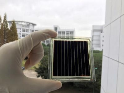
Researchers at Shanghai Jiao Tong University in China and the Swiss Federal Institute of Technology have reported the development of a new technique to deposit high-quality large-area perovskite films that does not require solvents or vacuum processing. The method reportedly produces homogeneous films with relatively few defects, which leads to an efficiency of 12.1% for a solar module made from a methylammonium lead halide film that is just over 36 cm2 in size.

The research team has developed a new technique to produce large-area methylammonium lead halide (CH3NH3PbI3) perovskite films that relies on rapidly converting amine complex precursors (CH3NH3I·mCH3NH2 (where m is close to 3) and PbI2·nCH3NH2 (where n is close to 1) to perovskite films and then applying pressure to them.
Furthermore, the pressure-processing step at the end is better than the spin-coating method that is widely employed for depositing perovskite films, according to the team.
The film produced by the new technique is highly uniform over a large area (36.1 cm2) with only a 2% variation in film thickness and the grains in the material are around 0.8-1.0 microns in size, which is three to four times bigger than those in spin-coated processed film. The researchers succeeded in making a photovoltaic module with a PCE of 12.1% from such a film.
According to the researchers, the technique will be useful for growing perovskite crystals, which could greatly reduce so-called trap states and further enhance the photovoltaic performance of these materials. 'It could be then used to produce low-cost optoelectronics devices, like light-emitting diodes or laser diodes on a large scale'.


