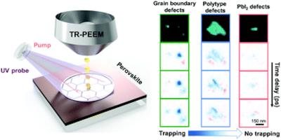
Researchers from the Femtosecond Spectroscopy Unit, led by Professor Keshav Dani, at the Okinawa Institute of Science and Technology Graduate University (OIST) and Optoelectronics Materials and Device Spectroscopy Group, led by Dr. Sam Stranks at the University of Cambridge, have identified three different kinds of defect clusters in perovskite thin films, which likely occur during fabrication and may impede efficiency of perovskite solar cells.

The perovskite material lies at the heart of the solar cell, which consists of many different layers. When the sun hits the solar cell, its energy is absorbed by the perovskite, causing electrons to jump into a higher energy level and leaving holes behind. All the electrons then move in one direction through the layers of the solar cell to the electrical contact and the holes, in the other direction, thus generating a current.
Defects that might impede efficiency are a known occurrence, but it was previously unclear whether these defects all had the same characteristics and could thus be removed using one strategy. In this study, by using state-of-the-art equipment, the defects were imaged and characterized with a nanoscale resolution to reveal three distinct kinds.
The most detrimental kind the researchers found was the grain boundary defect. These defects are tiny and, as the name suggests, sit at the boundary between different crystal grains of perovskite. They seemed to actively trap photogenerated holes and deplete efficiency from the regions far exceeding their size, thus causing huge issues for the performance of the perovskite.
Then there are polytype defects. These occur when the precursor material crystallizes, not in the typical cubic perovskite structure, but a hexagonal one. This type of defect cluster is relatively big and also negatively impacts efficiency by trapping photogenerated holes.
"If there are a lot of polytype defects in a film, their impact can become just as detrimental as the grain boundary ones," Sofiia explained. "Both the grain boundary and the polytype defects need to be targeted by developing specific strategies."
Finally, the study revealed the lead iodide defects. These form from precipitated lead iodide'an important part of perovskite material that is used during the fabrication. However, this research suggests that they seem to be benign in terms of trapping charges from perovskite and have little impact on efficiency.
The researchers decided to use an approach that is often used to reduce defect density in perovskites'treatment with light and oxygen'to see how these defects would respond. They did this by exposing the perovskite to visible light and a mildly oxygenated atmosphere. Interestingly, they found that the defects reacted in different ways. For example, the most detrimental grain boundary defects were healed and stopped trapping the holes. However, the effect on the other defect types was more nuanced and not necessarily beneficial.
"This research shows that we likely need targeted approaches to address the undesired effects of the different defect types, and thus improve the performance of perovskite solar cells," concluded Prof. Dani.

